All the latest quantum computer articles

See the latest stories on quantum computing from eeNews Europe

Friday, August 28, 2009

Imaging a molecule for the first time


Researchers at IBM in Zurich has managed to create accurate pictures of a molecule for the first time using non-contact atomic force microscopy (AFC).
The ability to image a molecule will help to open up atomic scale electronics, using molecules as switches an transistors.
“Though not an exact comparison, if you think about how a doctor uses an X-ray to image bones and organs inside the human body, we are using the atomic force microscope to image the atomic structures that are the backbones of individual molecules,” said IBM Researcher Gerhard Meyer. “Scanning probe techniques offer amazing potential for prototyping complex functional structures and for tailoring and studying their electronic and chemical properties on the atomic scale.”

The team’s current publication follows on the heels of another experiment published just two months ago in the June 12 issue of Science (Volume 324, Issue 5933, pp. 1428 – 1431) where IBM scientists measured the charge states of atoms using an AFM. These breakthroughs will open new possibilities for investigating how charge transmits through molecules or molecular networks. Understanding the charge distribution at the atomic scale is essential for building smaller, faster and more energy-efficient computing components than today’s processors and memory devices.
IBM Research – Zurich scientists Leo Gross, Fabian Mohn, Nikolaj Moll and Gerhard Meyer, in collaboration with Peter Liljeroth of Utrecht University, used an AFM operated in an ultrahigh vacuum and at very low temperatures (–268°C or – 451°F) to image the chemical structure of individual pentacene molecules. With their AFM, the IBM scientists, for the first time ever, were able to look through the electron cloud and see the atomic backbone of an individual molecule.
The AFM uses a sharp metal tip to measure the tiny forces between the tip and the sample, such as a molecule, to create an image. In the present experiments, the molecule investigated was pentacene. Pentacene is an oblong organic molecule consisting of 22 carbon atoms and 14 hydrogen atoms measuring 1.4 nanometers in length. The spacing between neighbouring carbon atoms is only 0.14 nanometers and in the experimental image, the hexagonal shapes of the five carbon rings as well as the carbon atoms in the molecule are clearly resolved. Even the positions of the hydrogen atoms of the molecule can be deduced from the image.
“The key to achieving atomic resolution was an atomically sharp and defined tip apex as well as the very high stability of the system,” recalls IBM scientist Leo Gross. “We prepared our tip by deliberately picking up single atoms and molecules and showed that it is the foremost tip atom or molecule that governs the contrast and resolution of our AFM measurements.”

A tip terminated with a carbon monoxide (CO) molecule yielded the optimum contrast at a tip height of approximately 0.5 nanometers above the molecule being imaged and—acting like a powerful magnifying glass—resolved the individual atoms within the pentacene molecule, revealing its exact atomic-scale chemical structure.
Furthermore, the scientists were able to derive a complete three-dimensional force map of the molecule investigated. “To obtain a complete force map the microscope needed to be highly stable, both mechanically and thermally, to ensure that both the tip of the AFM and the molecule remained unaltered during the more than 20 hours of data acquisition,” says Fabian Mohn, who is working on his PhD thesis at IBM Research – Zurich.

Reblog this post [with Zemanta]

Tuesday, August 25, 2009

Jukebox player startup thriving


Nice to see startups thriving. Martin Brennan, covered in my story in Electronics Weekly back in September 2007 is doing well with his JB7 jukebox that uses an innovative, simple interface to access thousands of CDs on a simple unit. The reviews are good and full page ads are appearing, so things are going well.

Reblog this post [with Zemanta]

Wednesday, August 19, 2009

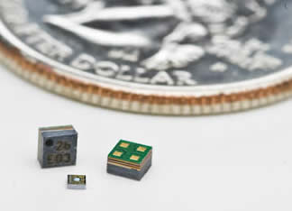
Silicon microphone moves to Bosch

Akustica, developer of silicon MEMS (micro electro-mechanical systems) microphones for the consumer electronics market has been bought by Robert Bosch North America. Terms of the agreement will not be disclosed.
Akustica, which was founded in 2001, is based in Pittsburgh, Pennsylvania and develops and sells digital and analogue micro electromechanical microphones using standard CMOS silicon technology. This approach allows the integration of transducer elements and associated integrated circuits on a single Silicon chip. Bosch is the world leader in MEMS sensors and, with this acquisition, further strengthens its position in this market.
“The strategic acquisition of Akustica with their outstanding application of sophisticated MEMS technology complements our growing semiconductor business and ideally complements our ongoing MEMS activities” said Dr. Stefan Kampmann, executive vice president, Bosch Automotive Electronics. “We look forward to working together with the Akustica team to continue to develop this important business area.”

To date Akustica, which developed and sold the world’s first digital MEMS microphone, has sold over 5 million microphones in the global market. All of the company’s 36 associates will be employed by Bosch.
According to Joseph A. Jacobson, president and chief executive officer, Akustica, Inc., “We are excited to join the market leader in MEMS sensors and be a part of Bosch's expansion in commercialization of consumer MEMS products. The strength of our combined technology, manufacturing capability, and talent will allow us to continue delivering innovative and differentiating sensor product solutions.”

Comment: However, this looks more like the inability of Akustica to raise more money in the current financial climate and not enough income to go it alone despite big early plans.

Reblog this post [with Zemanta]

Customer continuity is key says GE Fanuc

GE Fanuc has strongly objected to the idea that the joint venture has collapsed (see blog below), saying this is a strategic move based on changes in the market over the last twenty years. But it does not release turnover details for the joint venture, and with its focus on industrial and process control the joint venture is likely to be suffering as much as any other large equipment supplier.
The company does point to an amicable separation and the two parts will continue to work together to provide continuity for customers.

"The market place has changed, everything has changed since the joint venture was formed twenty three years ago," said a senior spokesperson at GE Fanuc. "One good example is the embedded business that is now a large part of GE. That's what is behind the dissolving, not the collapse, of the joint venture. This is a strategic decision so that both companies can refocus their interests for growth."
GE Fanuc acquired SBS Technologies, which had itself grown fast, and Radstone Technologies, in 2006, the latter for £130m, paying peak prices that I would expect not to be reflecting the same forward earnings in the current climate.
"This is not related to the downturn in the economy, but the downturn has made everyone focus on their business to see what they should focus on as the recovery occurs," said the spokesperson.

The two will continue to work together in motion control applications.
Comments?

Reblog this post [with Zemanta]

Wireless power standard emerges with logo


A standard for wireless charging of portable equipment is emerging through the Wireless Power Consortium. It has released the 0.95 technical specification for a global wireless power charging standard for low power devices that are 5 watts and below, such as mobile phones and personal music players. It is out for review by its members and announced the launch of prototype testing at a members' interoperability test to be held on 15-17 September, 2009.
The Consortium, established at the end of last year, has also chosen the logo “Qi” (pronounced “chee”, meaning “energy flow”) to represent the first international wireless power standard which brings new levels of convenience to power charging in consumer electronic devices.

“In just seven months the Wireless Power Consortium has advanced the standard to 0.95 for interoperability testing and moved to trademark “Qi” as the first universal wireless power standard. These significant milestones have been achieved through strong collaboration among the Consortium members and pave the way for an accelerated 1.0 release schedule of the standard,” said Camille Tang, Co-Chair of the Promotion Work Group at the consortium.

The interoperability test will be hosted in Eindhoven, The Netherlands, during the next Consortium meeting and is open to existing and new members joining prior to 15 September 2009.
In a recent survey by the consortium 90% of respondents said they would like to see a uniform symbol placed on electronic devices to indicate that the devices are equipped with wireless power charging. Under the consortium’s plans, all electronic devices bearing the “Qi” symbol can be charged on any charging pad or surface marked with the same “Qi” logo.


Full members:
ConvenientPower
Fulton Innovation
Logitech
National Semiconductor
Olympus
Philips
Sang Fei
Sanyo
Texas Instruments


ASSOCIATE MEMBERS

Duracell
Hosiden
Leggett & Platt
Samsung Electronics
ST-Ericsson
Reblog this post [with Zemanta]

Tuesday, August 18, 2009

Downturn hits as GE Fanuc splits

GE Fanuc Automation, the twenty year old joint venture between GE and FANUC, is to be dismantled by the end of the year. GE and FANUC expect the transaction to be completed by the end of this year, subject to satisfactory customary closing conditions. It denies the split is due to market conditions, see comments above.
Set up in 1986, GE Fanuc Automation serves a vast array of industries around the world including the energy, water, consumer packaged goods, government & defence, and telecommunications industries with hardware and software solutions, services, automation and embedded computing systems.
Under the terms of the agreement GE retains the software, services, embedded systems and control systems businesses globally. The company will be known as GE Intelligent Platforms, and will be led by GE Fanuc Intelligent Platforms CEO Maryrose Sylvester. FANUC retains the global CNC business.

FANUC Honorary Chairman Dr. Seiuemon Inaba said, “Our joint venture has achieved great success toward its original mission, which was to cooperate on the global growth and technical development of the PLC and CNC business. Over this time period, markets and opportunities also have changed dramatically, and both companies further expanded into adjacent segments. Today’s market conditions are such that it’s imperative we pursue these expanded opportunities, and while we have achieved great things together, it’s in both our best interests that we focus our efforts on industry opportunities unique to our respective companies and that will deliver greater benefits to both our companies.”

GE Fanuc Intelligent Platforms CEO Maryrose Sylvester said, "GE could not have asked for better partners than Dr. Inaba and FANUC. GE is proud of what our companies have achieved together - both the industry expertise and success across our product portfolios. For GE, this change will mean a continued, intense focus on serving our customers around the world while continuing to invest in significant growth platforms like process control systems, enterprise and automation software and embedded computing as we continue to build further expertise around the GE vertical infrastructure segments."
“Our top priority is a smooth completion of transition and continuity for all customers, business partners and employees. We are committed to delivering our customer commitments in every segment of our business."


Reblog this post [with Zemanta]

Friday, August 07, 2009

First European 1Gb/s Internet

Zon Multimedia in Portugal is planning to launch a 1Gbit/s Internet service in September, reports Julian Clover at Cable TV Europe and other sources.
This is a phenomenal rise in speeds, and will put pressure on other providers across Europe who have been talking about 100Mbit/s, which Zon launched in January.
The system, which runs over cable, has already been field tested.
These speeds will drive a whole new class of Internet connected services and devices over the next two to three years.

Reblog this post [with Zemanta]

Wednesday, August 05, 2009

Linux and Nucleus for Marvell Sheeva chip

Mentor Graphics has developed a combined open-source Linux and Nucleus operating system (OS) solution for the Marvell Sheeva MV78200 Dual-core Embedded Processor.
This dual operating system support was co-developed by Mentor and Marvell for low power devices such as network controllers, switches and routers, high-performance storage, enterprise printers, DVRs, NVRs and video surveillance, and high-volume SMB gateways.
“Our collaboration with Mentor Graphics’ embedded systems team has allowed Marvell to address the multi-OS needs of our customers using dual-core processors,” said Dr Simon Milner, vice president and general manager of the Enterprise Business Unit, Consumer and Communications Business Group at Marvell Semiconductor. “The performance and real time qualities of Mentor’s Nucleus OS complement the power and flexibility of Linux, while their tools and services give our mutual customers a boost in product development.”

The MV78200 is a dual-core, high-performance, low-power, highly-integrated processor with the Marvell Sheeva CPU cores. Built on Marvell’s innovative Discovery system controller platform, the MV78200 is a complete System-on-Chip (SoC) solution, optimized for low power operation and ideally suited to a wide range of applications ranging from sophisticated routers, switches and wireless base stations to high-volume laser printer applications. Developers can use the dual OSs to manage separate functional requirements, yet allow them to easily and reliably communicate with each other. Mentor’s Nucleus OS is a fast, scalable and deterministic OS that can be used for operational tasks such as those required in printing drums and ink coverage for enterprise printers, whereas the Linux OS would be used for user interaction and communication.

Reblog this post [with Zemanta]

China chip market booms


China's IC market is expected to reach $100.1 billion in 2013 and represent over one-third (35%) of the worldwide IC market, up from only 14 in 2003 (Figure 1) according to IC Insights Mid-Year Update to The McClean Report.
In 2001, the Asia-Pacific IC market (which includes China, Taiwan, Singapore, Korea, etc.) first surpassed the Americas segment (the U.S., Canada, Mexico, Central America, and South America) and became the leading IC-consuming market.
In 2008, the Asia-Pacific IC market was $111.2 billion, and, for the first time ever, was larger than the Americas, European, and Japanese IC markets combined!
The tremendous growth of the Asia-Pacific IC market over the past few years mirrors the trend toward increasing electronic system production in the Asia-Pacific region, especially in China. In general, regional IC market growth is typically closely matched to the growth of regional electronic system production.
With more of the world's electronic systems forecast to be produced in Asia-Pacific (non-Japan), and China in particular, IC Insights believes that Asia-Pacific IC market growth will continue to significantly outpace total IC market growth for at least the next five years.
In 2009, China and Taiwan together are expected to represent about 75% of the IC market in the Asia-Pacific region. In 2013, IC Insights forecasts that the China and Taiwan IC market together will reach about $139 billion and represent almost 80% of the total Asia-Pacific IC market and almost half (48%) of the worldwide IC market!
In 2008, China's IC market increased 5% to $56.2 billion as compared to a 6% decline for the total worldwide IC market. Although China's IC market is forecast to decline by 8% in 2009, this performance would still be much better than the 17% drop expected for the total IC market. Moreover, the Chinese IC market is forecast to have a 2008-2013 CAGR of 12%, double the 6% forecast for the worldwide IC market during this same time.

Tuesday, August 04, 2009

High speed 64Gbyte memory cards emerge

Looking back even a couple of years, the prospect of using a 64Gbyte memory card for storage would seem fantastic, but Toshiba is planning to ship such cards, using the latest SDXC standard, to OEMs in November.
The new SDXC and 32Gbyte and 16Gbyte SDHC Memory Cards are the world’s first memory cards compliant with the SD Memory Card Standard Ver. 3.00, UHS104, which brings a new level of high speed read and write speeds to NAND flash based memory cards: a maximum write speed of 35MByte per second, and a read speed of 60MByte per second. For example, it would be possible to download 2.4GB video data in only 70 seconds.
SDXC Memory Card is the next-generation SD Memory Card standard defined by the SD Association in April 2009, in order to meet the ever-growing demand for high-capacity memory media, offering higher transfer rates for content rich storage applications. The new SDXC Memory Card Standard applies to cards with capacities over 32GB and up to 2Terabytes compared to the SDHC standard, which applies to cards with capacities from 4GB to 32GB. Like the move from SD to SDHC, the new cards are only compatible with SDXC readers, not existing SDHC systems.
UHS 104 is the new ultra high speed interface that delivers data at a rate of 104MB/ sec. It is the highest standard in the new SD Memory Card Standard Ver. 3.00.


Reblog this post [with Zemanta]

Wireless test and virtualisation for LabView 2009


National Instruments has launched its the latest version of the LabView graphical system design software platform for test, control and embedded system development. LabVIEW 2009 simplifies the development challenges of complex test systems with new tools that streamline the software engineering process for the development, deployment and maintenance of critical test software. It uses parallel programming features such as virtualisation technology that increase the performance for multicore-enabled test applications and offers LabVIEW FPGA compiler improvements to simplify field-programmable gate array (FPGA) reconfigurable I/O (RIO) development. In addition, LabVIEW provides new solutions for testing systems based on wireless standards such as WLAN, WiMAX, GPS and MIMO using a common hardware platform.
“In today’s challenging economic climate, engineers and scientists are being asked to complete their projects with fewer resources and in less time,” said Dr. James Truchard, President, CEO and Cofounder of National Instruments. “With LabVIEW 2009, test engineers can develop complex and mission-critical applications faster while improving their overall test system performance.”

Streamline Test Software Validation
LabVIEW 2009 features new tools for software engineering and code validation that make it possible for engineers and scientists to easily meet the regulatory and software engineering requirements of complex test systems. With the new version of LabVIEW, engineers and scientists can trace the implementation of test system requirements to virtual instrument (VI) programs and easily monitor low-level details about the execution of critical VIs for quick application monitoring and debugging. In addition, LabVIEW 2009 can automate the functional testing of each VI to guarantee that the VIs meet all necessary specifications. These new software engineering tools complement existing LabVIEW features for large application development and help engineers and scientists create high-quality test systems.
Improve Parallel System Development
With LabVIEW 2009, engineers and scientists can easily develop applications that take advantage of inherently parallel technologies such as FPGAs and multicore processors. Virtualisation technology makes it possible to run multiple OSs side by side on the same multicore processing hardware to build more efficient systems. Using new NI Real-Time Hypervisor software, engineers and scientists can run Windows XP and LabVIEW Real-Time OSs side by side on the same PXI embedded controller and partition the processor cores among the two OSs for more efficient use of system resources.
The LabVIEW 2009 FPGA Module also further reduces the time required to program FPGA RIO devices by providing early compile feedback and critical path highlighting during compilation and simulation on a development computer. This helps engineers and scientists make early FPGA resource usage estimates and better debug timing violations. They also can further reduce development time by simulating the behavior of an FPGA on a development computer instead of compiling to the FPGA.
Test More Wireless Devices and Standards
LabVIEW 2009 improves the performance of radio frequency (RF) and wireless test by taking advantage of multicore processors. For example, engineers and scientists can use LabVIEW and off-the-shelf multicore processors to increase the speed of wireless measurements such as spectral masks and error vector magnitude used in WLAN test. The recently released NI WLAN Measurement Suite for LabVIEW guarantees compliance with IEEE 802.11 a/b/g standards and performs measurements more than five times faster than traditional box instruments. With software-defined instrumentation using LabVIEW, engineers and scientists can implement the same measurement platform to generate, analyse and simulate nearly any wireless standard or custom protocol. In addition to the WLAN Measurement Suite, the recently released WiMAX, GPS and MIMO tools for LabVIEW help engineers and scientists increase their performance when testing multiple standards using a common PXI hardware platform.

Reblog this post [with Zemanta]

Sunday, August 02, 2009

Google data on spring cleaning solar panels

Google has been looking at whether it should clean its solar panels, and d'uh, finds that the efficiency rises dramatically when it does! However, there are also some interesting slides on the data they collected.

Ever since we assembled a 1.6 MW solar panel installation at our headquarters in Mountain View in 2007, we've been wondering, "Does cleaning the solar panels make them more effective?" We thought it might, but we needed to be sure. So we analyzed the mountains of data that we collect about the energy that these panels produce — after rain, after cleaning and at different times of the year.

We have two different sets of solar panels on our campus — completely flat ones installed on carports, and rooftop ones that are tilted.

Since the carport solar panels have no tilt, rain doesn't do a good job of rinsing off the dirt they collect. (Also, our carports are situated across from a sand field, which doesn't help the situation.) We cleaned these panels for the first time after they had been in operation for 15 months, and their energy output doubled overnight. When we cleaned them again eight months later, their output instantly increased by 36 percent. In fact, we found that cleaning these panels is the #1 way to maximize the energy they produce. As a result, we've added the carport solar panels to our spring cleaning checklist.

The rooftop solar panels are a different story. Our data indicates that rain does a sufficient job of cleaning the tilted solar panels. Some dirt does accumulate in the corners, but the resulting reduction in energy output is fairly small — and cleaning tilted panels does not significantly increase their energy production. So for now, we'll let Mother Nature take care of cleaning our rooftop panels.

Accumulated dirt in the corners of a rooftop solar panel

We've also been crunching numbers on dollars-and-cents; the more energy our panels produce, the sooner we'll be paid back by our solar investment. Our analysis now predicts that Google's system will pay for itself in about six and a half years, which is even better than we initially expected.

If you want to learn more about our solar study, check out these slides showing the effects that seasonality, tilt, dirt, particulate matter, rain and cleaning have on Google's solar energy output. We hope you solar panel owners out there can tailor our analysis to the specifics of your own installation to produce some extra energy of your own!


Reblog this post [with Zemanta]