All the latest quantum computer articles

See the latest stories on quantum computing from eeNews Europe

Wednesday, January 31, 2018

JEDEC doubles SD card speeds, adds 2.5V and MIPI support to Universal Flash Storage and UFS Card Extension specs

By Nick Flaherty www.flaherty.co.uk

The JEDEC Solid State Technology Association has published the latest version of its  Universal Flash Storage (UFS) and Card Extension specifications for the latest embedded mobile and computing designs as well as automotive.

UFS 3.0 JESD220D is the first standard to introduce MIPI M-PHY HS-Gear4 with a data rate of up to 11.6 Gbps per lane, twice the performance increase over prior versions of the specification, and includes 2.5V support. It also includes two features introduced specifically for the automotive market: the ability to function at an extended temperature range and refresh operation. 

UFS is a high-performance interface designed for use in applications where power consumption needs to be minimised. The high-speed serial interface and optimized protocol enable significant improvements in throughput and system performance.  

Version 3.0 references the MIPI M-PHY v4.1 physical layer specification and the recently released MIPI UniProSM v1.8 transport layer specification as well as: 
  • 2.5V Vcc power supply enables lower power consumption and support for the latest NAND technology
  • Temperature event notification, including device alert based on a pre-defined temperature range
  • RPMB Regions, supporting multiple Replay Protected Memory Block (RPMB) keys with multiple associated RPMB regions. RPMB regions are fixed at manufacturing and are now also configurable at manufacturing to allow secure areas of memory.
  • Device Error History: Logging mode defined for the device to enable in-system debugging
  • Extended temperature range (-40C, 105C) and refresh operation with added host control mechanism to improve device data reliability in automotive designs
The JESD223 UFS Host Controller Interface (UFSHCI) version 3.0 standard is intended to simplify the design process by defining a standard host controller interface. This allows system designers to create a common host controller software driver to work with UFS host controller hardware from different manufacturers. The HCI functionality enables higher performance and power efficiency by minimizing the involvement of the host processor in the operation of the Flash storage subsystem. 

JESD223D is designed to use Adapt support in MIPI M-PHY v4.1 and QoS support defined in the recently released MIPI UniPro v1.8 specification to support more reliable link communication by monitoring and training the communication channel.

UFS Card Extension version 1.1 includes minor updates and editorial changes, including full support for HS-G1/G2/G3 and the addition of power definition for the card, RMS and peak.

“UFS 3.0, UFSHCI 3.0 and the UFS Card Extension update offer a host of enhancements over the prior versions of these standards that will help product designers enable significant improvements in mobile devices and related applications,” said Mian Quddus, Chairman of the JEDEC Board of Directors and the JC-64 Committee for Embedded Memory Storage and Removable Memory Cards. He added, “The addition of features specifically for the automotive market underscores the commitment of JEDEC members to continue to evolve the UFS ecosystem to meet the needs of the industry and, ultimately, the consumer.”

JESD220D, JESD223D and JESD220-2A are available for download from the JEDEC website. at www.jedec.org.

Related stories:

Friday, January 26, 2018

Skyworks teams with Broadcom on 802.11ax

By Nick Flaherty www.flaherty.co.uk

Broadcom is using an integrated high power transmit and low-noise receive amplification module from Skyworks for its latest 802.11ax wifi reference designs. 

The 2.4 and 5.0 GHz 802.11ax modules and Broadcom’s Max WiFi processors provide four times faster download speeds, six times faster upload speeds, enhanced coverage and up to seven times longer battery life when compared to 802.11ac wifi designs today.
“Skyworks is excited to be collaborating with Broadcom to combine our advanced connectivity engines with their sixth generation wifi devices,” said David Stasey, vice president and general manager of diversified analog solutions for Skyworks. “This strategic partnership gives our customers a unique opportunity to deliver best-in-class wireless experiences for consumers across many new markets spanning multimedia streaming, autonomous cars and augmented/virtual reality.”

Next generation 802.11ax devices are starting to be adopted across the consumer electronics industry, as companies throughout the ecosystem begin developing solutions and products in support of the new standard. End applications for the Max WiFi modules include Wi-Fi routers, residential gateways, enterprise access points, and client devices. One of the key benefits of the 802.11ax standard is that it allows for a more robust and dedicated connection with data-intensive applications such as 4K TV, particularly when multiple users are streaming Wi-Fi simultaneously.

According to ABI Research, 802.11ax devices will account for 57 percent of wifi chipsets by 2021.

More information about Skyworks’ 802.11ax solutions can be found on its Wi-Fi Connectivity page and as part of Broadcom’s maxwifi.org or BCM43684 and BCM43694 reference designs.

Google launches 'drag and drop' machine learning in the cloud

By Nick Flaherty www.flaherty.co.uk

Google has launched a drag and drop development system for cloud-based machine learning (ML) to simplify the implementation of artificial intelligence (AI) systems. As we have said consistently, linking embedded system to these capabilities both at the edge and in the cloud is driving the roll out of effective networks in the Internet of Things (IoT).

The problem is that currently, only a handful of businesses in the world have access to the talent and budgets needed to fully appreciate the advancements of ML and AI. There’s a very limited number of people that can create advanced machine learning models, and the process is still time-intensive and complicated to build a custom ML model. While Google has offered pre-trained machine learning models via APIs that perform specific tasks, there's still a long road ahead.

Cloud AutoML uses techniques like learning2learn and transfer learning to help huild ML models for machine vision, helping AI experts be even more productive and less-skilled engineers build powerful AI systems.

The first Cloud AutoML release will be Cloud AutoML Vision, a service that makes it faster and easier to create custom ML models for image recognition. The drag-and-drop interface lets developers  upload images, train and manage models, and then deploy those trained models directly on Google Cloud. Early results using Cloud AutoML Vision to classify popular public datasets like ImageNet and CIFAR have shown more accurate results with fewer misclassifications than generic ML APIs.

Cloud AutoML Vision is built on Google’s leading image recognition approaches, including transfer learning and neural architecture search technologies for a more accurate model in minutes to pilot an AI-enabled application, or for a full, production-ready model in as little as a day. It provides a simple graphical user interface that lets designers specify data, then turns that data into a customised model. 

Related stories:

Thursday, January 25, 2018

Industry's first 400Gbit/s DSP with integrated laser drivers targets cloud data centres

By Nick Flaherty www.flaherty.co.uk

MaxLinear has launched the industry's first 400Gbit/s pulse-amplitude-modulation (PAM4) digital signal processing (DSP) systems-on-chip (SoC) that include integrated electro-absorption modulated laser (EA-EML) drivers to drive a new generation of high speed optical interconnects

The MxL935XX Telluride family is a key component for system designers to develop a 400Gbit/s optical interconnect module in a compact form factor for intra-datacentre applications with a transmission distance up to 2km.

The 16nm CMOS chip consumes an extremely low power of 6.7W, which includes the integrated EA-EML driver power dissipation. This meets the stringent power constraints of 400Gbits optical module form-factors such as QSFP-DD, OSFP and COBO devices.

MaxLinear is currently sampling the device to optical module vendors who are actively developing 400Gbit/s modules that are expected to enter mass production in the latter half of 2018.

The chip supports of one, two or four lanes of 100Gbit/s optical connectivity combined with a flexible 25G NRZ and 50G PAM4 electrical interface supporting multiple generations of switch ASICs. This means it can be used in a wide-range of optical interconnects supporting 100Gbit/s, 200Gbit/s and 400Gbit/s optical fibre data speeds in cloud mega-scale and enterprise data centres.

The integrated laser drivers directly interface with the external optical lasers and eliminate the need for expensive external high-frequency components required for laser driver and modulator bias.

"The exploding data traffic, and the demand for high-speed data have placed an enormous burden on the cloud and enterprise data network infrastructure. This is, in turn, not only compressing the network upgrade cycle, but is also accelerating the need to deploy 400Gbit/s optical networks inside mega-scale cloud and enterprise data centers," said Dr. Kishore Seendripu, CEO of MaxLinear. "With the recent announcement of the availability of next-generation switch ASICs that support 50Gbit/s PAM4 I/Os, we believe the growth trajectory for PAM4 DSP-based 400Gbit/s optical fibre interconnect solutions is at an inflection point. The cost pressure and thermal constraints of 400Gbit/s networks necessitate the use of new optical interconnects based on single-lane 100Gbit/s optical wavelength technology.

"Our Telluride MxL935XX 16nm CMOS SoC family, with integrated EA-EML laser drivers, reduced external components, and superior link-margin performance, is perfectly positioned to enable this leapfrogging industry transition. We believe that, currently, the total addressable market for 100Gbit/s and 400Gbit/s optical interconnect modules greatly exceeds 10 million units annually, not including the anticipated future rapid growth driven by the exploding internet traffic," he said. 

The first SoCs to be available from the Telluride family are the MxL93542 and MxL93543, which feature several operating modes that can connect to multiple generation of switch ASICs (128x25G NRZ, 256x25G NRZ or 256x50G PAM4) enabling 3.2Tbit/s, 6.4Tbit/s or 12.8Tbit/s front panel capacity per data centre rack unit. These different operating modes span a variety of optical module form factors such as QSFP28, SFP-DD, QSFP-DD, OSFP and COBO.

For modes where the MxL93542 and MxL93543 interface with a legacy 25G NRZ switch ASIC, the corresponding forward error correction (FEC) functionality required for PAM4 optics is integrated into the device. Two separate instantiations of the FEC engine are available on-chip to support two distinct lanes of 100Gbit/s optics.

The integrated laser driver in the MXL93542 delivers greater than 1.8V of single-ended driver output swing necessary for EA-EML lasers. This output swing easily meets the optical modulation amplitude (OMA) specification requirements across the wide operating temperature and bias ranges of all EA-EML lasers. The chip package also includes all the high frequency components required for driver & modulator biasing.

The second version of the SoC, the MxL93543, delivers 800mV of peak-to-peak differential driver output swing and can be easily paired with an external laser driver implemented in alternate optical technologies such as silicon photonics.

The devices feature a comprehensive digital pre-distortion (DPD) engine in the transmit direction to compensate for laser non-linearity, and to cancel packaging limitations that cause reflections and bandwidth degradation at these extremely high signal frequencies. On the receive path, the DSP includes an auto-adaptive signal enhancement engine, which integrates a continuous time linear equalizer (CTLE), automatic gain control (AGC), a feed forward equalizer (FFE), and a decision feedback equalizer (DFE).

The MxL93542 and MxL93543 are sampling now to optical module manufacturers. 


Industry set to ship 1 trillion chips this year

By Nick Flaherty www.flaherty.co.uk

The semiconductor industry is set to ship over 1 trillion devices this year, from integrated circuits to opto-sensor-discretes.

The market is set to grow 9% in 2018 to 1,075.1bn, according to the latest IC Insights’ McClean Report. The volume shipments are driven by sensors, accounting for 70% of total semiconductor units compared to 30% for ICs.


Over the span of just four years (2004-2007), semiconductor shipments broke through the 400-, 500-, and 600-billion unit levels before the global financial meltdown caused a big decline in semiconductor unit shipments in 2008 and 2009. Unit growth rebounded sharply with 25% growth in 2010 and displayed another strong increase in 2017 (14% growth) to climb past the 900-billion level.

The largest annual increase in semiconductor unit growth during the timespan shown was 34% in 1984, and the biggest decline was 19% in 2001 following the dot-com bust. The global financial meltdown and ensuing recession caused semiconductor shipments to fall in both 2008 and 2009; the only time that the industry experienced consecutive years in which unit shipments declined. The 25% increase in 2010 was the second-highest growth rate across the time span.

 Thirty-eight years ago in 1980, O-S-D devices accounted for 78% of semiconductor units and ICs represented 22% (Figure 2).


Semiconductor products forecast to have the strongest unit growth rates in 2018 are those that are essential building-block components in smartphones, automotive electronics systems, and within systems that are helping to build out of Internet of Things. 

The fastest growing categories for 2018 include the industrial sector with a 26% increase in analogue devices, a 22% growth in dedicated chips for consumer designs and a 21% growth in 32bit microcontrollers. Analogue devices for wireless communication are set for 18% growth while analogue for automotive will see 17% growth. Among O-S-D devices, CCDs and CMOS image sensors, laser transmitters, and every type of sensor product (magnetic, acceleration and yaw, pressure, and other sensors) are expected to enjoy double-digit unit growth this year.
Related stories:

Wednesday, January 24, 2018

Hardware virtualised GPU core for automotive infotainment designs

By Nick Flaherty www.flaherty.co.uk

Despite all the upheaval around its ownership, Imagination Technologies has launched a new high performance GPU core that supports the multiple, ultra-high resolution displays for cluster, Head-Up Display (HUD) and infotainment. 

The Furian GPU architecture provides an 80% higher fill rate density than the previous generation, allowing the four-cluster PowerVR Series8XT GT8540 GPU to simultaneously drive up to six 4K screens with complex UIs at 60fps.

The PowerVR graphics technology now represents the core of Imagination's business so it is good to see continuing technology development.

The hardware virtualisation can provide a complete separation of services and applications, ensuring they remain secure against system intrusion or data corruption. The platform can support up to eight applications or services running in separate containers at once and automotive OEMs can deploy and remove services at will without affecting others running at the same time.

As more in-car infotainment systems move towards richer operating systems such as Android and CarPlay (despite Imagination's very public falling out with Apple), the importance of a GPU capable of full hardware virtualisation to contain rogue apps is of increasing importance. Allowing a rich graphical environment for the infotainment system while protecting the dashboard and other critical displays will be unaffected by malware enables higher levels of system integration, reducing costs, whilst maintaining the safety critical requirements of the design.

The Series8XT GT8540 can support long-running compute workloads on a single Shader Processing Unit (SPU) for ADAS functions such as lane departure warning, blind-spot detection, and surround view, amongst others. Other tasks, such as infotainment and cluster, can run on the second SPU, using prioritising mechanisms to reach system performance targets.

“With the PowerVR Series8XT GT8540 Imagination Technologies continues to prove that it is a leader in the automotive space," said Dominique Bonte, Managing Director and Vice President, ABI Research. "As the automotive industry moves closer to introducing Level 4 and Level 5 autonomous vehicles, powerful GPUs will be vital to power multiple high-resolution display. With distraction concerns removed in driverless cars, additional opportunities for advanced infotainment features including 5G-based 4K video streaming will emerge in the longer term. Imagination is in a strong position to support this progression. The ability to run multiple workloads over each SPU is a potential game changer for the automotive industry.”

“PowerVR has a strong roadmap and this is reflected in the great success seen with the XT family and its selection by leading automotive players, such as Texas Instruments. We’re now targeting new markets with the rich features, such as safety and security through virtualisation,” said Graham Deacon, Vice President PowerVR Marketing, Imagination Technologies.

The PowerVR Series 8XT GT8540 is now ready for licensing. The PowerVR two-cluster Series8XT GT8525 has customers in segments including automotive and mobile.

Tuesday, January 23, 2018

First look at Nordic's Cortex M33 cellular IoT module

By Nick Flaherty www.flaherty.co.uk

Nordic Semiconductor has demonstrated its nRF91 Series low power cellular module for the Internet of Things based around the new ARM Cortex M33 core. The module can run on the Verizon Wireless Network in the US and on the Telia network in Norway.


The nRF91 Series is intended to bring the simplicity of wireless LAN technology to cellular IoT architectures. In much the same way as Nordic Semiconductor's nRF5 Series enabled innovation and drove adoption of Bluetooth wireless technology in new markets, the nRF91 Series is designed to be an easily accessible solution for cellular connectivity.

The nRF91 Series is a highly-integrated, low power, global multimode LTE-M / NB-IoT System-in-Package (SiP) that integrates a complete low power cellular IoT system in 10x16x1.2mm package. This includes modem, transceiver, RF front end, dedicated application processor, Flash memory, power management, and crystal and passive components.

Qorvo as a strategic partner for both the RF front end and the SiP development and manufacturing and the module uses Qorvo’s RF front-end, advanced packaging, and MicroShield technology to get the small footprint. It supports global operation with a single SiP variant thanks to the combination of Nordic’s multimode LTE-M / NB-IoT modem, SAW-less transceiver, and a custom RF front-end.

The module uses ARM's Cortex-M33 host processor, along with TrustZone security and Assisted GPS. This is the first embedded core based on ARM's v8 instruction set.
 
The nRF91 takes security for low power IoT devices to new heights by combining the inherent security of cellular connectivity with additional security for the application hardware and software. The integration of an Arm Cortex-M33 processor and Arm CryptoCell-310 security IP enables an entire low power cellular IoT application to be implemented on an nRF91 SiP.

The built-in host processor features TrustZone for Armv8-M, helping secure application data, firmware, and peripherals using an isolated, trusted execution environment across the CPU and system. This provides an efficient security foundation, and reduces size, Bill-of-Materials (BOM), and power consumption versus using an external host processor.

The nRF91 also features built-in support for positioning via an integrated Assisted GPS (A-GPS) solution that combines cellular and GPS technology to deliver fast and accurate positioning.
Jointly developed by Nordic’s highly experienced cellular design team in Finland, and low power experts in Norway, the chip was developed from scratch to optimise the power, cost, and size savings enabled by the new LTE-M and NB-IoT cellular standards. The chip features an unprecedented and unique level of integration by combining a multimode cellular modem and transceiver, as well as application processor, Flash memory, RAM memory, and power management on a single chip.

It includes a complete suite of software and easy-to-use development tools to accelerate innovation and product development with a thriving Nordic development community. This all combines to allow developers to concentrate on developing their own products and services using cellular technology.

“Back in early 2015, when we started the development of nRF91 Series, we set out on a mission to create a truly different solution for cellular IoT,” said Thomas Embla Bonnerud, the Director of Strategy and Investor Relations at Nordic Semiconductor. “A highly integrated, low power, ultra-compact, and simple-to-use solution that would foster innovation and accelerate adoption of cellular connectivity across new markets. We are confident that the upcoming nRF91 Series represents such different solution, and we are excited to provide a sneak peek and demonstration of it today.”

“We are pleased with our strategic partnership with Nordic to bring this new category of cellular IoT solution to the market,” said Eric Creviston, President Mobile Products at Qorvo. “Qorvo is excited to see our leading RF and advanced packaging technology playing a key and enabling part of new products targeting the emerging low power cellular IoT market.”

“Delivering the combination of power efficient, TrustZone secure, and cellular connectivity capabilities to the extensive Cortex-M developer base opens up the benefits of IoT to a diverse range of new and innovative applications,” said Thomas Ensergueix, Senior Director of Embedded, Embedded and Automotive Line of Business, Arm. “We are pleased to see the nRF91 SiP from Nordic with Cortex-M33 and CryptoCell-310 enabling the deployment of secure IoT solutions at scale.”

Nordic is sampling nRF91 to selected lead customers now. Start of general sampling is planned for mid-2018, with first production quantities available by end of 2018. The nRF91 SIP will be available in variants with and without integrated GPS.

Sunday, January 21, 2018

Fully embedded stand-alone Wi-Fi module for highly integrated applications

By Nick Flaherty www.flaherty.co.uk

Panasonic Industry Europe has launched a fully embedded stand alone Wi-Fi module for highly integrated and cost-effective applications.

The PAN9420 device is a 2.4GHz 802.11 b/g/n fully embedded Wi-Fi Module with integrated stack and API that minimises firmware development and includes a full security suite. It is based around the 88MW300 system-on-chip from Marvell which uses a 200MHzARM Cortex M4F microcontroller core with a flash controller and 32Kbytes of SRAM cache for execute in pace (XIP) applications and updates. 


A fully shielded case, integrated crystal oscillators and a chip antenna allows the PAN9420 module to combine the 88MW300, high-sensitivity wireless radio, baseband processor, medium access controller, encryption unit, boot ROM with patching capability, internal SRAM and in-system programmable flash memory. The integrated memory enables storing web content such as HTML pages or image data while the parallel support of access point and infrastructure mode allows easy setup of simultaneous Wi-Fi connections from the PAN9420 to smart devices and home network routers. 

The pre-programmed Wi-Fi SoC firmware enables Ad-hoc mode (Wi-Fi Direct) applications. With the transparent mode, raw data can be sent from the UART to the air interface to smart devices, web servers or PC applications.

Also now available is a PAN9420 Evaluation Kit containing a motherboard with PAN9420 daughter board (PAN9420 FCC version module) which easily connects to any PC using the USB-cable included. The motherboard comes with two USB to UART converters allowing for hardware access to the two UART module interfaces (command and binary interface). The PAN9420 FCC version module comes pre-loaded with a firmware for IoT applications and a Panasonic Web content example.
The PAN9420 module is available in two version: FCC/IC (P/N: ENW49C01A3KF) and CE RED (P/N: ENW49C02A3KF) pre-certified.

https://eu.industrial.panasonic.com/sites/default/pidseu/files/downloads/files/wm_pan9420_datasheet_0.pdf

Related stories:

Thursday, January 18, 2018

Graphene sensors target the IoT

By Nick Flaherty www.flaherty.co.uk

Researchers at The University of Manchester have developed graphene sensors embedded into RFIDs, which they say have the potential to revolutionise the Internet of Things (IoT).

Layering graphene-oxide over graphene creates a flexible structure for a a humidity sensor with the ability to connect to any wireless network as part of an RFID system.

Such sensors can be printed layer-by-layer for scalable and mass production at very low cost. The device also requires no battery source as it harvests power from the receiver. This can be used for various applications such as battery-free smart wireless monitoring for manufacturing processes that are sensitive to moisture, food safety, healthcare and nuclear waste.

"The excitement does not end with this new application here, but leads to the future possibilities of integrations of this technique with other 2D materials to open up a new horizon of wireless sensing applications," said Dr Zhirun Hu who led the work.

This is the first example of the printable technology where several 2D materials come together to create a functional device immediately suitable for industrial applications.


Tuesday, January 16, 2018

Remote monitoring and control over Ethernet and wireless for IIoT

By Nick Flaherty www.flaherty.co.uk

Acromag has teamed up with California-based Ctek for a complete monitoring and control system to manage remote assets in the Industrial Internet of Things (IIoT). 

The deal combines Acromag's signal measurement and conditioning products with Ctek's expertise in cellular communication and autonomous controllers for a distributed control system without all the integration hassles. Users can quickly and cost-effectively deploy these systems without programming to connect endpoints to the enterprise, enabling visual access to operation status from anywhere. Menu-based configuration speeds setup of data collection, reporting, and alarm functions.
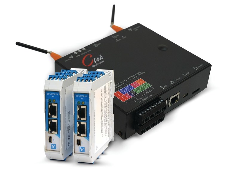
Acromag BusWorks Ethernet I/O Modules and Ctek 4G/LTE SkyRouter Controller


The integrated Acromag/Ctek system is intended for remotely monitoring and controlling the operation of pumps, motors, tanks, meters, generators, batteries, valves, fans, heaters, and other industrial equipment. Users can rapidly set up data displays, alarm rules, data logging and process control logic routines with point-and-click application development. Controllers support wired serial, Ethernet, and 4G/LTE network communication plus a cloud-based application service for easy access to critical system status reporting.

The Ctek SkyRouter controllers provide autonomous intelligence and sophisticated communication capabilities to manage operations and report performance data. They operate as a Modbus master to read and write to slave I/O devices. Powerful processing capabilities include thresholds, math/boolean functions, triggers, data logging, and much more. Alarms support email and SMS messaging.

Acromag BusWorks® remote I/O modules interface analogue and discrete level sensors. The multi-channel I/O modules convert voltage and current signals representing temperature, level, flow, load, on/off, high/low, and other performance measures to Modbus values. Rugged design, hazloc approvals, and isolated signal processing ensure high-accuracy, reliable performance in harsh locations.

"With this joint solution from Acromag and Ctek, customers can reliably monitor and control remote automation equipment without the hassles of PLC programming or IT networking issues," said Robert Greenfield, Acromag's Business Development Manager.

"Now system developers can confidently pair Acromag I/O and Ctek controllers to rapidly implement SCADA solutions with cloud-based reporting that are affordably scalable for small and large sites," observed Bob Way, Ctek's Business Development Manager.

www.acromag.com

Telit certifies LTE Cat-M1 module for IoT with Telstra

By Nick Flaherty www.flaherty.co.uk

Telit has certified its quad-band, dual-mode ME910C1-AU, based on the Qualcomm MDM9206 LTE IoT modem, for LTE Category M1 (Cat M1) operation on Telstra's mobile network. 

The certification means IoT integrators and providers looking to deploy in Australia can quickly start taking advantage of the reliability and around three million square kilometers of Telstra's LTE Cat M1 coverage built specifically for the IoT. 

"This certification is a first in many ways for Telit," said Yosi Fait, Telit CEO. "The ME910 is the first to receive Telstra Cat M1 certification; it is the first regional market launch of the dual-mode Cat M1 and NB1 module series of the ME910C1; and it is the first IoT module form-factor in Australia available for all commercially available cellular standards in the region. With it, our existing customers integrating or selling products into Australia using 2G or 3G modules from the xE910 family, can now simply drop in the new ME910C1-AU and start testing Cat M1 in a matter of weeks. New projects can also get to market quickly with assistance from our network of customer support centres and distributors available in the same time zone with local presence in a number of metropolitan areas in Australia."

The ME910C1-AU module is a pin-to-pin replacement for existing devices based on the family's modules for 2G, 3G, LTE Categories 1, 3 and 4. Developers can cut costs and development time by simply designing for the xE910 LGA common form factor, giving them the freedom to deploy technologies best suited for the application's environment. The ME910C1-AU also features optimised power consumption and optional quad-constellation GNSS support capabilities.

The longevity of the LTE Cat M1 standard and extensive feature set make it an ideal solution for new and existing applications in vertical segments like telematics, smart energy and metering, asset tracking, retail, point-of-sale, security and surveillance, industrial control and automation, smart home, and smart buildings.

info.telit.com/nbiot

Related stories:

Scalable deep neural network AI accelerators for edge processing

By Nick Flaherty www.flaherty.co.uk


Hua Xia GPT (hxGPT), China's leading licensor of customisable processor IP cores, has developed a family of scalable, programmable AI accelerators. The cores range from handset to edge processing for a wide range of applications including the Internet of Things (IoT), Advanced Driver Assistance Systems (ADAS), Self-driving Cars, Robotics, Surveillance, and Machine Vision.

The "Song" AI core is a highly configurable IP block that provides for efficient implementations of CNN's. Running at up to 1GHz in 28nm technology, each accelerator core contains 288 MAC units scalable to beyond 2 TFLOPS. Performance, power, and size can be optimised for low power embedded IoT devices and edge processing designs. 

Accuracy can be optimised using built-in 16-bit integer or floating point operations. Support for compressed 8-bit data is provided. Extended precision intermediate results reduce errors in both regression and classification workloads.

Targeting inference applications, the AI accelerator supports multi-dimensional tensor processing. The design provides direct support for convolution, pooling, dropout, padding, and programmable activation functions. A library of popular CNN networks is provided with general framework support such as Tensorflow and Caffee is in development.

Previously hxGPT announced availability and licensing of the Changcheng out-of-order superscalar CPU. This has been tested in TSMC's 28nm process, the core is configurable providing for multiple performance levels based on customer requirements. Memories, caches, and out-of-order features (issue window, ROB, rename, etc.) can all be customised. Depending upon technology selection the core can run up to 3GHz at very low power.

The Song AI core integrates with the Changcheng CPU for ease of programming. Both are programmed using the same proprietary processor programming environment.

WuxiDSP, hxGPT's customer of both the Changcheng core and Song AI core, has used them for  silicon that is scheduled to sample later this year targeting edge IoT processing, says Xiaodong Zhang, Chief Engineer of WuxiDSP.

hxGPT is the only IC design house in China with a portfolio of proprietary intellectual property for CPU, DSP, GPU and AI accelerators targeted at high-end SoC designs for heterogeneous computing. The company has 8 issued patents and more than 90 pending world-wide patents covering the core architecture and implementations of the next generation processor design. It has operations in New York, Beijing, and Shanghai.

www.GeneralProcessorTech.com

Related stories:

Monday, January 15, 2018

Power news this week

By Nick Flaherty www.flaherty.co.uk

Automated fault injection without changing source code

By Nick Flaherty www.flaherty.co.uk

German embedded software test tool developer Razorcat has developed a automated fault injection capability for its unit and integration test tool TESSY, version 4.1 or higher. Test cases with fault injections can be generated and managed easily and implemented in unit tests, integration tests and component tests automatically without changing the source code – saving time and money.


In practice, whenever the necessary code coverage of 100% cannot be reached with normal test cases, fault injections are applied manually by adding testing code or code replacements using compiler macros, by replacing functions (stubbing) or by changing variable values using debug tools. These methods have the disadvantage that they need to be done either manually or that the instrumentation of the source code remains in place within production code. The test engineer is usually the first to realise the need for a fault injection. If the code needs to be changed, all necessary approvals of software development according to safety standards need to be performed again. Such an iteration highly increases development time and cost.


In TESSY 4.1, however, fault injection is automated and does not remain in the source program. The error injections are defined directly in the flow chart of the function within the TESSY environment.

Test cases with automated fault injection have a special flag and will be documented within the test report. When all test cases are executed, these special test cases can be included or excluded from the test execution. All fault injections are conveniently stored and managed in TESSY. This means fault injections can be assigned to one or more test cases in a user-friendly way and will be effective at the desired location even after source code changes when doing regression testing.

The automated fault injection will be shown in the new TESSY version 4.1 at embedded world 2018 in February

Wireless sensor hub evaluation kit for real time data in the IoT and Smart Home

By Nick Flaherty www.flaherty.co.uk

Integrated Device Technology (IDT) has launched an evaluation kit for its wireless sensor hub which allows product designers and engineers to connect high-performance humidity, temperature and flow sensors in their latest industrial IoT, smart home, connected appliances, fluid metering and control and environmental monitoring applications.

The SDAWIR0x development environment integrates IDT's HS3001 humidity and temperature sensor, FS2012 flow sensor and ZWIR4512 6LoWPAN module and network stack in a single sensor module. The ZWIR4512 connects the environmental sensors via Wi-Fi to output the sensor data in real-time to a private network where it can be viewed on iOS or Android devices. Up to one hundred of these sensor modules can be connected to a single Wi-Fi hub; or thousands in a full mesh network. 

Over-The-Air (OTA) firmware updates simplify development and system updates after deployment. This flexible platform makes the SDAWIR0x ideal for a wide variety of connected devices requiring real-time temperature, humidity and flow data, such as smart thermostats, smart refrigerators, environmental weather stations, pumps and metering equipment and medical infusion pumps and CPAPs.

"The SDAWIR0x uniquely combines our 6LoWPAN solution – which is already proven in smart home and municipal lighting networks – with our royalty-free security stack and OTA update capabilities to provide engineers an industrial-strength development platform for a wide range of IoT, connected home, smart appliance and other applications," said Sailesh Chittipeddi, IDT's executive vice president for global operations and chief technology officer.

Wirelessly updating the SDAWIR0x's firmware is simple and straightforward thanks to the device's OTA update capability. This includes integrity checking and failure recovery mechanisms to ensure it will not become unusable even in case of error.

The SDAWIR0x security stack enables secure, end-to-end communication – even over unsecure network nodes – with its standard-compliant implementations of the Internet Protocol Security (IPSec) protocol suite and the Internet Key Exchange Protocol version 2 (IKEv2).

Friday, January 12, 2018

Intel posts details of speculative execution vulnerability

By Nick Flaherty www.flaherty.co.uk

Intel has posted its detailed response to the Meltdown and Spectre vulnerabilities in its processors.

"As detailed by Google Project Zero, a new series of side-channel analysis methods have been discovered that potentially facilitate access to unauthorised information," said the company. "These methods rely on common properties of both high-performance microprocessors modern operating systems and susceptibility is not limited to Intel processors, nor does it imply the processor is working outside its intended functional specification. All of the methods take advantage of speculative execution, a common technique in processors used to achieve high performance. Intel is working closely with our partners, as well as with other silicon vendors whose processors are affected, to design mitigations for these methods."

The issues are detailed in a white paper along with the techniques used to stop the data being accessed.

www.intel.com

Segger launches portable embedded web server, adds HTTPS support

By Nick Flaherty www.flaherty.co.uk

Tool developer Segger has commercialised its internal embedded web server to provide a browser interface to any kind of device, service or software module for easy monitoring.This is a key way of provisioning devices in the Internet of Things but needs a very efficient implementation. 

The emWeb web server, used by the company for its own products, is written entirely in C to easily integrate into any existing application on embedded devices, tablets / cell phones or host computers running Windows, Linux or macOS. This means that the device or application can be monitored and controlled in real time from any other device using a browser, no application needs to be provided to the end customer, engineering efforts can be kept to a minimum.

emWeb uses HTTP, a widely established standard, as the underlying base for the user interface. This makes it very portable and accessible. The only requirement is a browser, no drivers are needed to support access on any operating system. The user interface can be scaled depending on resources and requirements from traditional basic HTML to modern interfaces using Javascript, Ajax, SSE, Websockets and more.

This can be combined with Segger's emSSL TLS product for HTTPS secure links. Minimal configuration with a single connection would use 7k of ROM code, or 4k RAM without SSL, so there's no reason not to.

Even devices without traditional interfaces, such as Ethernet or WiFi are able to make use of the universal user interface provided by emWeb. With IP-over-USB technology, Segger provides a state-of-the-art solution for USB devices to be configured, accessed, and monitored through a universal browser UI. Design only a single UI that will work on any end user device.

emWeb has a very small memory footprint for embedded devices, even resource constrained single-chip, microcontroller based devices, and the company uses this technology in many of its own products, such as the J-Link, the J-Link PC software, the Flasher and Flasher ATE products.

Thursday, January 11, 2018

Synopsys forms Technical Advisory Board for embedded software integrity

By Nick Flaherty www.flaherty.co.uk

Synopsys has appointed a Technical Advisory Board (TAB) to guide the technical direction of its  Software Integrity Group’s security products and services.

Despite being a synthesis tool provider, hardware IP and embedded software has been a major part of the company's growth, particularly for applications such as automotive and the Internet of Things. 

The five-member board of experienced software and security executives will advise Synopsys on broader trends in the software industry, provide input on its solutions strategy, and help align its priorities with the requirements of its customers and market.

“Delivering exceptional value to our customers through innovative, cutting-edge solutions is core to our business,” said Andreas Kuehlmann, general manager of the Software Integrity Group. “Though our staff already includes many of the world’s premier software security experts, we understand it is important to build and maintain an objective outside perspective to review and augment our technical strategies. The TAB members, made up of accomplished technologists, will help us do this.”

The TAB will be chaired by Dr. Gary McGraw, vice president of security technology at Synopsys. The initial board members include Dr. Brian Chess (Oracle), Dr. Neil Daswani (Symantec), Dr. Charlie Miller (Cruise Automation), and Dr. Laurie Williams (North Carolina State University).
The Software Integrity Platform unites leading testing technologies, automated analysis, and experts to create a robust portfolio of products and services. This portfolio enables companies to develop personalised programs for detecting and remediating defects and vulnerabilities early in the development process, minimising risk and maximising productivity. 

ADRF teams with Sirqul to layer cellular data over the IoT

By Nick Flaherty www.flaherty.co.uk

Distributed Antenna System developer Advanced RF Technologies is working with SIoT provider Sirqul to incorporate data from the cellular connections ADRF provides.

ADRF has joined the Sirqul's Strategic Alliance Partner Program to incorporate data from 3G and 4G and add redundancy to Sirqul's IoT network.

"Sirqul has created a strong technology offering that allows its customers to draw real-time and location-based insights from IoT data," said Greg Najjar, Director, Business Development of ADRF. "Joining the Strategic Alliance enables ADRF to become a critical component of Sirqul's solution and bring 'smart' experiences to more venues."

Sirqul offers software and mesh networking technology to track and identify individuals' behaviour, location, and intent. This can range from identifying the exact whereabouts of a fan at a sports stadium to deliver food to enabling autonomous robots to navigate industrial warehouses and factories, as well as be monitored.

ADRF's technology enables Sirqul to create new opportunities for venues and buildings that aren't equipped to provide WiFi. Through the partnership, Sirqul will be able to use ADRF's expertise in deploying successful wireless solutions and mission-critical technologies in public arenas, apartment complexes, smart buildings, and professional sports stadiums to enhance their platform offering.

"ADRF has deployed thousands of implementations in the same markets as Sirqul's client base, including stadiums and arenas, retailers, and other commercial properties," said Viki Zabala, Chief Marketing Officer of Sirqul. "Through this partnership, we're able to rapidly expand our capabilities to easily connect infrastructure to customer engagement for our clients."

ADRF is the latest addition to the Strategic Alliance Program, which includes companies such as Intel, Siemens, and Level 11. 

Wednesday, January 10, 2018

Toshiba's first Bluetooth 5 chips trade data rate for range

By Nick Flaherty www.flaherty.co.uk

Toshiba has launched two new Bluetooth 5 chips with a longer range at the 125kbit/s data rate.
As a result the TC35680FSG (featuring built-in flash memory) and TC35681FSG are aimed at applications requiring long-range communication, including beacon tags, IoT devices and industrial equipment. Sample shipments will begin later this month.

The chips support the full spectrum of data rates required for the high-speed features – 2M PHY and Coded PHY (500kbit/s and 125kbit/s) – Bluetooth 5.0 standard but trade off the data rate to get the sensitivity for the longer range. The chips have a receiver sensitivity level of -105dBm at 125kbit/s compared to -94.5dBm at 1Mbit/s, but do have a built-in power amplifier in the transmission block that provides up to +8 dBm transmission power for longer range (down to -40dBm for lower power consumption).

The chips are based on an ARM Cortex-M0 processor with a 256KB Mask ROM to support the Bluetooth baseband process and 144KB of RAM for processing Bluetooth baseband, stack and data. They have 18 ports of GPIO which can be set to 2 channels each for SPIs, I2C, and UART. This allows for the structuring of systems that connect to various peripheral devices. These GPIOs can be set for a wakeup function, 4-channel PWM, 5-channel AD converter interfaces, an external amplifier control interface for long-range communication, and more.

The TC35680FSG includes 128KB of flash memory for storing user programs and various data in stand-alone operations, removing the need for external non-volatile memory. This also lowers the part count, which reduces both the cost and mounting area.

The TC35681FSG, which does not include a built-in flash memory, operates in conjunction with an external non-volatile memory or host processor. A wide operating range of -40° to +125°C makes it suitable for applications exposed to high temperatures.

The power consumption is 11.0mA operating at 3.0V, +8dBm and 1Mbit/s for the transmitter and 5.1mA for the receiver at 3.0V  and 1Mbit/s, with a 100nA current at 3.0V in Deep Sleep

It supports Bluetooth low energy Ver. 5.0 central and peripheral devices and has built-in GATT (Generic Attribute Profile), supporting servers and clients defined by GATT.

Tuesday, January 09, 2018

Entry level FPGA WiFi dev board supports RISC-V Soft CPU

By Nick Flaherty www.flaherty.co.uk

Microsemi has teamed up with distributor Future Electronics on a low cost development board that uses a Microsemi PolarFire non-volatile field programmable gate array (FPGA) with a RISC-V soft core.

The Avalanche development board includes a RISC-V-based soft central processing unit (CPU) pre-programmed to the kit (for replacing MIPS designs) alongside WiFi and Ethernet networking. This supports the ongoing expansion of Microsemi's recently announced Mi-V ecosystem, which brings together industry leaders involved in the development of RISC-V to leverage their capabilities and streamline RISC-V designs for customers. 
As the lowest cost entry development board available today for designing with Microsemi's lowest power, cost-optimised mid-range PolarFire FPGAs, Future's Avalanche board lowers the barrier to entry for PolarFire FPGAs (from the Actel acquisition) and helps expand Microsemi's market opportunities for the device.

"The availability of Future Electronics' Avalanche board delivers customers the best value for a mid-range density FPGA development board featuring our PolarFire FPGAs," said Ted Marena, director of FPGA marketing for Microsemi. 

"With 300K logic elements (LEs), a Wi-Fi module, 1000 Base-T and numerous expansion connectors, engineers can quickly prototype their ideas at minimal cost. Future Electronics has not only lowered the cost to adopt PolarFire FPGAs, but it is also enabling customers to develop solutions leveraging the power of Microsemi's Mi-V ecosystem and the open RISC-V ISA," he said.

Future Electronics' Avalanche development board also features serial flash memory, double data rate type three (DDR3) DRAM and a Microsemi VSC8531 triple speed PHY powered by Microsemi's LX7167 2.4A hysteretic step-down regulator, making the platform ideal for developing several applications within the industrial market, including industrial internet of things (IoT), secured wired communications, Gb Ethernet bridging and imaging. It also offers industry-standard connectors Arduino Shield, mikroBUS and a Peripheral Module (Pmod) interface. These three expansion headers allow for the use of additional boards to implement an expanded set of applications including infrared, thermal imaging, industrial cameras, touch screen and other wireless interfaces.

"As the newest addition to our family of development boards, the Avalanche board offers the lowest cost platform available in the market for Microsemi's innovative PolarFire technology," said Martin Bernier, director of the Engineering Support Group for Future Electronics. "We believe industrial, medical, defense and communication customers will be excited about PolarFire FPGA's ability to deliver up to 50 percent lower power than other mid-range density devices."

The increasing cost of manufacturing applications with specific input/outputs (I/Os) and interfaces means producing application-specific integrated circuits (ASICs) and processors optimized for every device scenario is becoming unsustainable. This is especially true as both IoT and artificial intelligence (AI) drive interconnect and networking complexity. In many markets, especially wired communications, industrial and automotive, FPGAs and other configurable logic solutions are increasingly relied on to fill the gap--solving throughput, security and interface challenges, while their flexibility drives down overall cost associated with supporting product line diversity. Because of this, Tom Hackenberg, embedded processors principal analyst at IHS Markit, predicts strong renewed FPGA growth in these markets with a compound annual growth rate (CAGR) ranging from just under 6 percent to over 10 percent from 2016 to 2021.

Microsemi's PolarFire FPGA devices provide cost-effective bandwidth processing capabilities with the lowest power footprint. They feature 12.7 Gbps transceivers and offer up to 50 percent lower power than competing mid-range FPGAs, and include hardened PCIe controller cores with both endpoints and root port modes available, as well as low power transceivers. The company's PolarFire Evaluation Kit is a comprehensive alternative platform for evaluating its PolarFire FPGAs which includes a PCIe edge connector with four lanes and a demonstration design. The kit features a high-pin-count (HPC) FPGA mezzanine card (FMC), a single full-duplex lane of surface mount assemblies (SMAs), PCIe x4 fingers, dual Gigabit Ethernet RJ45 and a small form-factor pluggable (SFP) module.

The Avalanche board for PolarFire, part number AVMPF300TS-01, is available now from Future Electronics. 


Related stories:

Monday, January 08, 2018

IAR boosts development of FreeRTOS IoT module

By Nick Flaherty www.flaherty.co.uk

Tool vendor IAR is supporting the new WiFi-based IoT module from NXP.

The module is based around the LPC54018 microcontroller and includes support for Amazon FreeRTOS and provides a seamless Wi-Fi connection to Amazon Web Services (AWS), enabling developers to create secure, cost-effective IoT solutions. 

The module offers unlimited memory extention, a root of trust built on the embedded SRAM physical unclonable functions (PUF) and on-chip cryptographic accelerators. The software libraries of Amazon FreeRTOS mean cloud on-boarding and over-the-air device management is simplified and theIAR Embedded Workbench provides code optimisation technology and extensive debugging functionality.

The speed optimisations and IAR C/C++ Compiler generate fast, efficient code for high-performance, low-power applications. To enable extensive debugging and profiling, the toolchain includes features such as complex code and data breakpoints, runtime stack analysis, call stack visualisation, code coverage analysis and integrated monitoring of power consumption. Through add-on tools for static analysis and runtime analysis, developers gain complete code control.

“We recently announced support for the new IoT microcontroller operating system Amazon FreeRTOS from Amazon Web Services,” said Anders Lundgren, Product Manager at IAR Systems. “This support in combination with the powerful code optimizations and debugging capabilities of IAR Embedded Workbench will enable developers to leverage the full potential of the new IoT module from NXP.”

More information about IAR Embedded Workbench for Arm is available at www.iar.com/iar-embedded-workbench/tools-for-arm/.

Related stories: