By Nick Flaherty www.flaherty.co.uk
Anti-virus developer Avast is tapping into visitor’s phones at Mobile World Congress in Barcelona this year to highlight the vulnerability of devices to mining cryptocurrencies. Nearly 60,00 devices in the city are potentially vulnerable.
It is also planning to launch its own hardware hub to protect smart home networks, and was using this as an example of how cryptojacking works.
Initial research by Avast shows that an army of more than 15,800 devices would be needed to mine $1,000 in Monero coins over the four days of the congress. Smartphones and IoT devices, like smart TVs or webcams or thermostats, often have very low computation power, which is bad for mining. For this reason, cybercriminals are looking to attack devices at a mass scale to maximize profit. Mining on IoT devices remains largely invisible to the consumer; unlike a PC, it’s not as noticeable when an IoT device heats up or loses performance.
“Until recently, cybercriminals were focused on spreading malware to turn PCs into crypto-mining machines, but now we are also seeing an uptick in attacks targeting IoT devices and smartphones,” said Gagan Singh, Senior Vice President and General Manager, Mobile, at Avast. “According to current data from Shodan.io, 58,031 smart devices in Barcelona are vulnerable. If each of these devices were recruited to a botnet to mine Monero at Mobile World Congress, cybercriminals could earn the approximate equivalent of $3,600, or €3,000. The costs involved in mining are so high that profit from cryptocurrency mining is very low, encouraging cybercriminals to not attack tens of thousands but millions of devices.”
Last year the first IoT botnet appeared, a new version of the Mirai botnet emerged to mine cryptocurrencies. Since then, the risk of cybercriminals taking control of IoT devices to profit from cryptocurrency mining has increased.
The demonstration of mining was to highlight its new tool called Smart Life to address IoT security threats that will also come with a smart hub device. This uses machine learning to identify and block threats and is delivered through a Software-as-a-Service (SaaS) model to service providers and customers.
“It has been five years now since the first well-publicized hack of a baby monitor in Texas. Since then, IoT devices have transformed our homes and workplaces, but the security of these connected devices has not been significantly improved and users are still at risk. We increasingly expect convenience and enjoyment from smart devices like smart speakers, smart doorbells or IP cameras, but with this rapid adoption comes a real urgency to address the complex challenge of protecting them,” said Gagan Singh, Senior Vice President and General Manager of Mobile at Avast.
“With over 400 million active users worldwide at Avast, we get unparalleled insights into how IoT devices work which feed our cloud-based machine learning engine to identify and quickly block anomalies, botnets and other threats to IoT devices. When developing the Smart Life platform to harness the power of this technology, our focus was on delivering a security service that is easy for people to use to secure all of their IoT devices and networks,” he said.
Many smart devices can be compromised, including thermostats, streaming boxes, webcams and digital personal assistants. One of the more common types of attack is when cybercriminals hack thousands of IoT devices in unsuspecting households to create botnets to perform attacks on others.
One of Avast’s initial offerings based on the Smart Life platform, Avast Smart Home Security, will provide protection and visibility into what is happening on their home network. Key features include the detection of privacy threats, botnets and malware as well as safe browsing and prevention of Distributed Denial of Service (DDoS) attacks.
For example if a smart heating thermostat is turned on at an unusual time and is transmitting data in high volume to an unknown location, then Avast can instantly take action to shut down the attack and alert the family to the activity. This will be available later this year through a mobile app along with a hub that connects to the home network.
www.avast.com
Related stories:

Wednesday, February 28, 2018
Trinamic to build motion control chips with RISC-V core
By Nick Flaherty www.flaherty.co.uk
Eating into the MIPS business, embedded motor and motion control chip maker Trinamic has selected the Bk3 processor from Czech designer Codasip for its next designs. The Bk3 is based on the open source RISC-V architecture.
German Trinamic’s products serve multiple markets including laboratory and factory automation, semiconductor manufacturing, textiles, robotics, ATMs, and vending machines – wherever reliable positioning is required such as 3D printing, medical pumps, and security cameras.
“We chose RISC-V as the microcontroller platform for our future motion control product families. The open source character of the instruction set ensures the longevity our customers require,” stated Jonas P. Proeger, Marketing Director of Trinamic. “After investigating alternatives, we determined that Codasip’s Bk3 offered the ideal combination of performance and power efficiency that our applications demand. Backed by best-in-class development tools and the RISC-V ecosystem, the Bk3 is perfect for our future processing needs”.
The Codasip Bk3 processor, based on the RISC-V open instruction set architecture (ISA) definition, features a single 3-stage in-order execution processor pipeline and offers optional caches, IEEE 1149.1 debug, and industry standard bus interfaces. Further, the Bk3 – like all Codasip RISC-V implementations – is fully configurable and extensible, offering great advantage over traditional, fixed-configuration processor IP cores.
www.trinamic.com and www.codasip.com
Tuesday, February 27, 2018
Kerlink and Semtech test out non-GPS location technology in Mexico
By Nick Flaherty www.flaherty.co.uk
IoT network provider Kerlink is working with LoRa chip supplier Semtech to test out urban non-GPS location technology in Aguascalientes City, Mexico.
Live tests in the demonstration show promising results with CEP 95 (circular error probable with 95 percent probability) around 80m for moving objects, such as vehicles, in class A type of communication while in urban environments that can create communication multipath challenges, resulting from radio reflection generated by buildings.
Semtech, whose LoRa devices and wireless radio frequency technology transceivers are central to the implementation of LoRaWAN networks around the world, actively collaborated with Kerlink on equipment installation in Aguascalientes City, a metropolitan area of about 1 million population.
“Optimal location of the gateways is crucial for delivering an optimized, fine time stamp for real-time tracking,” said Marc Pegulu, vice president and general manager of Semtech’s Wireless and Sensing Product Group. “Kerlink’s Wirnet iBTS Compact, based on Semtech’s industrial-grade reference design, offers improved gateway clock synchronization for its embedded GPS to further improve geolocation accuracy, especially in a dense urban area.”
The urban environment will also help the teams to further evaluate network and gateway-deployment geometry, which plays a significant role in geolocation performance. All of these findings will help Kerlink continuously optimize the network design and deployment it offers customers through its professional services, including geolocation services.
”The global performance of the accuracy is continuously progressing by leveraging environment learning and intelligent algorithms,” Delibie said. “The infrastructure set-up is an alive technical ecosystem of partners delivering the entire value chain with a tremendous improvement in the quality of service able to support an increasing number of concrete use cases.”
Land-based geolocation using the LoRaWAN open protocol uses a different technology than GPS, eliminating the requirement for costly and power-hungry data processing. Gartner forecasts that a third of the world’s 15 billion connected devices will be critically dependent on geodata by the end of 2020.
The Mexican project is the first demonstration of Kerlink’s end-to-end network environment, which combines the Wirnet iBTS 915 MHz gateways, the Wanesy Management Center, which is the company’s core network management suite, and the Wanesy Geolocation, its new geolocation solver. The experiment with Semtech provides large-scale field-testing opportunities to demonstrate the benefits of geolocation and to show the impact of the quality of coverage on accuracy, when the number of gateways and location of installation points is varied in a dense urban setting.
“Geolocation is simple to deploy and operate because each end-device can be natively located without the need to add a costly GPS module inside it,” said Yannick Delibie, Kerlink CTIO. “This dramatically optimizes power consumption and reduces device hardware costs. No additional hardware is required, assuming that gateways are geolocation-ready."
Semtech, whose LoRa devices and wireless radio frequency technology transceivers are central to the implementation of LoRaWAN networks around the world, actively collaborated with Kerlink on equipment installation in Aguascalientes City, a metropolitan area of about 1 million population.
“Optimal location of the gateways is crucial for delivering an optimized, fine time stamp for real-time tracking,” said Marc Pegulu, vice president and general manager of Semtech’s Wireless and Sensing Product Group. “Kerlink’s Wirnet iBTS Compact, based on Semtech’s industrial-grade reference design, offers improved gateway clock synchronization for its embedded GPS to further improve geolocation accuracy, especially in a dense urban area.”
The urban environment will also help the teams to further evaluate network and gateway-deployment geometry, which plays a significant role in geolocation performance. All of these findings will help Kerlink continuously optimize the network design and deployment it offers customers through its professional services, including geolocation services.
”The global performance of the accuracy is continuously progressing by leveraging environment learning and intelligent algorithms,” Delibie said. “The infrastructure set-up is an alive technical ecosystem of partners delivering the entire value chain with a tremendous improvement in the quality of service able to support an increasing number of concrete use cases.”
Semtech and Kerlink are among the founding members of the LoRa AllianceTM, which recently published a white paper on geolocation using Semtech’s LoRa technology.
NXP launches i.MX IoT-on-a-Chip for Edge Computing
By Nick Flaherty www.flaherty.co.uk
NXP has developed an IoT-on-a-chip device that compbines an ARM-based i.MX applications processor, Wi-Fi and Bluetooth into small footprint with security and connectivity.
IoT-on-a-Chip brings together the pre-integrated features from NXP’s i.MX applications processor family and Wi-Fi/Bluetooth solutions for consumer and industrial developers to quickly build compact IoT products. It uses an Arm Cortex-A7 applications processor with dual-band 802.11ac Wi-Fi and Bluetooth 4.2 as a reference Wi-Fi certified module with proven Wi-Fi/BT software stacks.
Different levels of i.MX performance in the same 14x14 body size, using the same inter-chip interface. Footprint compatible top-modules provide a range of Wi-Fi/BT options suited to your application.
“Representing a major step in the evolution from on-board offerings to the future vision of IoT-on-a-Chip, our highly integrated solution completely demystifies the Internet of Things,” said Martyn Humphries, vice president of i.MX applications processors for industrial and consumer markets with NXP. “NXP’s forward-looking design approach will provide customers with far greater efficiencies across their systems, allowing them to accelerate their time to market for products – at no additional cost.”
NXP’s first IoT-on-a-Chip product, based on the i.MX 6ULL applications processor, will be available in late 2018. i.MX 7 and i.MX 8 processor configurations will be available in 2019.
NXP has developed an IoT-on-a-chip device that compbines an ARM-based i.MX applications processor, Wi-Fi and Bluetooth into small footprint with security and connectivity.
IoT-on-a-Chip brings together the pre-integrated features from NXP’s i.MX applications processor family and Wi-Fi/Bluetooth solutions for consumer and industrial developers to quickly build compact IoT products. It uses an Arm Cortex-A7 applications processor with dual-band 802.11ac Wi-Fi and Bluetooth 4.2 as a reference Wi-Fi certified module with proven Wi-Fi/BT software stacks.
The i.MX applications processors provide advanced security implementation for secure boot, tamper detection and response, and high throughput cryptography, and the IoT-on-a-chip can be expanded with its custom inter-chip interface to include a secure element without increasing the package footprint
The 14mm x 14mm x 2.7mm solution includes applications processor and Wi-Fi/BT in a single footprint and the package design allows DDR memory direct connect via pass-through board layout simplifies PCB design and provides additional space savings.
Different levels of i.MX performance in the same 14x14 body size, using the same inter-chip interface. Footprint compatible top-modules provide a range of Wi-Fi/BT options suited to your application.
“Representing a major step in the evolution from on-board offerings to the future vision of IoT-on-a-Chip, our highly integrated solution completely demystifies the Internet of Things,” said Martyn Humphries, vice president of i.MX applications processors for industrial and consumer markets with NXP. “NXP’s forward-looking design approach will provide customers with far greater efficiencies across their systems, allowing them to accelerate their time to market for products – at no additional cost.”
NXP’s first IoT-on-a-Chip product, based on the i.MX 6ULL applications processor, will be available in late 2018. i.MX 7 and i.MX 8 processor configurations will be available in 2019.
Monday, February 26, 2018
Power news this week
By Nick Flaherty www.flaherty.co.uk

POWER NEWS
 . Magnet for electric motors cuts rare earth use by half
 . TE teams for 25,000 digital component models
 . Five energy trends for 2018
 . Power trends: Fab plans for ultracapacitor material startup
 . OXIS investment opens up Brazilian R&D centre
POWER TECHNOLOGIES TO WATCH
 . Wireless charging a smartphone with a laser
 . Experimentation and quantum computation identifies solid oxide fuel cell materials
 . Power scheme boosts optical interconnect performance in data centres
NEW POWER PRODUCTS
 . 200V high current photorelay targets AC circuits
 . Power connectors boost density with 60A/blade and AC options
TECHNICAL PAPERS
 . National Instruments: Architectures for implementing a hardware-in-the-loop testing system
 . Software Defined Radio Handbook, 13th Edition
 . Clever lighting: an emerging new market
POWER NEWS
. Magnet for electric motors cuts rare earth use by half . TE teams for 25,000 digital component models . Five energy trends for 2018 . Power trends: Fab plans for ultracapacitor material startup . OXIS investment opens up Brazilian R&D centrePOWER TECHNOLOGIES TO WATCH
. Wireless charging a smartphone with a laser . Experimentation and quantum computation identifies solid oxide fuel cell materials . Power scheme boosts optical interconnect performance in data centresNEW POWER PRODUCTS
. 200V high current photorelay targets AC circuits . Power connectors boost density with 60A/blade and AC optionsTECHNICAL PAPERS
. National Instruments: Architectures for implementing a hardware-in-the-loop testing system . Software Defined Radio Handbook, 13th Edition . Clever lighting: an emerging new marketADLINK demos first true fog computing
By Nick Flaherty www.flaherty.co.uk
ADLINK Technology is set to demonstrate true Fog Computing for the first time later this week.
The system includes not only device monitoring, but also the management of the orchestration of embedded devices, all the edge of the Internet of Things (IoT).
The demonstration is based on ADLINK’s prototype open source Fog Computing platform (code-named fog∅5) that provides the end-to- end virtualization of compute, storage and
communication resources from Cloud services to connected embedded devices.
The demonstration is based on ADLINK’s prototype open source Fog Computing platform (code-named fog∅5) that provides the end-to- end virtualization of compute, storage and
communication resources from Cloud services to connected embedded devices.
ADLINK will also demonstrate its implementation of SGeT’s Universal IoT Connector (UIC) specification as a plug-in to the fog05 platform. Together, fog05 and SGeT/UIC go well beyond providing standard device connectivity to bring true Fog Computing to embedded computing.
“We’re very pleased to be able to demonstrate true Fog Computing,” said Angelo Corsaro, CTO of ADLINK. “Also our developments in UIC connectivity and XRCE data communications give our embedded computing customers a good view of the future and thus opportunities to plan for their next-generation IoT solutions. For ADLINK, Edge Computing is connected-embedded- computing, so pioneering seamless connectivity solutions from Cloud Services to Fog Nodes to embedded systems (also known as Fog Computing) is a strategic priority for us.”
www.adlinktech.com
www.adlinktech.com
Friday, February 23, 2018
Adesto XiP boosts battery life in ST's IoT nodes
By Nick Flaherty www.flaherty.co.uk
Adesto Technologies has teamed up with STMicroelectronics for low-power, low-latency eXecute-in-Place (XiP) operation on ST’s STM32L4+ microcontrollers.
“By pairing ST’s new ultra-low power STM32L4+ MCUs with EcoXiP, designers can architect high-performance, low-power XiP systems for more energy-efficient, lower-cost products,” said Gideon Intrater, CTO of Adesto. “Not every application needs a XiP solution, but for those that can benefit from it, there is no better solution in the market than EcoXiP.”
Samples of Adesto’s EcoXiP non-volatile system-accelerating memory are available now in densities from 32Mbit to 128Mbit.
Adesto Technologies has teamed up with STMicroelectronics for low-power, low-latency eXecute-in-Place (XiP) operation on ST’s STM32L4+ microcontrollers.
The combination of STM32L4+ MCUs and Adesto's EcoXiP non-volatile memories enables designers to create IoT devices requiring numerous sensors and other advanced capabilities with longer battery life.
The STM32L4+ series adds more embedded memory and connnectivity, and is the first STM32-family architecture to have two Octal SPI ports which support NOR Flash including XiP operation.
For many applications, the embedded memory in an MCU is not sufficient, and external XiP memory provides a solution.
“By pairing ST’s new ultra-low power STM32L4+ MCUs with EcoXiP, designers can architect high-performance, low-power XiP systems for more energy-efficient, lower-cost products,” said Gideon Intrater, CTO of Adesto. “Not every application needs a XiP solution, but for those that can benefit from it, there is no better solution in the market than EcoXiP.”
Samples of Adesto’s EcoXiP non-volatile system-accelerating memory are available now in densities from 32Mbit to 128Mbit.
Thursday, February 22, 2018
mbed launches certified IoT modules
By Nick Flaherty www.flaherty.co.uk
mbed, the online embedded development tool supplier, has expanded its Mbed Enabled program to include production modules pre-verified to support the Mbed OS operating system and associated connectivity protocols. The program provides product developers with a simple entry point to the marketplace, where they can find mass production quality modules running high quality open source software and supporting a diverse suite of connectivity drivers and protocols.


mbed, the online embedded development tool supplier, has expanded its Mbed Enabled program to include production modules pre-verified to support the Mbed OS operating system and associated connectivity protocols. The program provides product developers with a simple entry point to the marketplace, where they can find mass production quality modules running high quality open source software and supporting a diverse suite of connectivity drivers and protocols.
IoT system makers are turning to module manufacturers to provide pre-verified functionality, particularly for host-less modules featuring an onboard microprocessor and built in connectivity. With so many vendors and modules to choose from, selecting the most suitable module vendor with the right experience and scale to support the company’s specific requirements has become a significant barrier to entry.
Additionally, due to the range of connectivity options used in IoT, finding a cross platform software solution with professional development tools is also problematic. Product developers often repeat costly software development programs when developing product families that must support a range of connectivity standards.
The Mbed Enabled Module program is being launched now with wiFI, Bluetooth and LoRa modules from u-blox, Advantech and Multitech running mbed OS.
u-blox ODIN-W2
- Dual Band Wi-Fi (2.4 and 5 GHz)
- Cortex-M4 with FPU, 168 MHz
- 2MB Flash, 256kB RAM
Multitech Dragonfly
- mbed deployable product
- Cortex-M4 + Cellular Radio
- FCC and Carrier Certified
Multitech xDOT
- LoRaWan 1.0.1 Compliant
- Cortex-M3 32MHz, 256kB flash
- 2uA current draw in low power
u-blox NINA-B1
- Bluetooth low energy v5.0
- Cortex-M4 with FPU, 64 MHz
- Fully certified module
Advantech WISE-1570
- ARM Cortex-M4 Core Processor
- 3GPP R14 NB-IoT Compliant
- Integrated with Mbed Cloud
Multitech Dragonfly Nano
- End device certified by carriers
- Low power modes
- Family of cellular options
Advantech WISE-1530
- ARM Cortex-M4 Core Processor
- Integrated Wi-Fi and BT4.1
- Rich interface for sensors
Advantech WISE-1510
- ARM Cortex-M4 Core Processor
- Built-in LoRa / LoRaWAN
- Rich interfaces for sensors
Related stories:
- Semtech delivers LoRaWAN IoT networking via ARM's mbed dev tool
- mbed OS 5.7 brings robust embedded file management and mesh networking stack
Murata teams with Altair and ST on smallest CAT-M/NB1 IoT module
By Nick Flaherty www.flaherty.co.uk
Murata is using Altair Semiconductor's dual-mode CAT-M1/NB1 chipset and STMicroelectronics' STM32 MCU and ST33 Secure MCU for a new generation of cellular IoT modules and end nodes devices.
"The CAT-M/NB1 module with GNSS will be the world's smallest form factor solution enabling new possibilities and applications that were not possible before. Additionally, their simplicity and high level of integration will drastically reduce time to market," said Mehul Udani, General Manager, Connectivity Solutions at Murata
The ALT1250 chipset powers Murata's Type 1SE end device and Type 1SC module, supports CAT-M1 and NB1 narrowband communications over existing cellular 4G networks. It incorporates Altair's OneSKU RF technology to enable multiple LTE band combinations, as well as CAT-M1 and NB1 functionality with a single hardware design.
Murata is using Altair Semiconductor's dual-mode CAT-M1/NB1 chipset and STMicroelectronics' STM32 MCU and ST33 Secure MCU for a new generation of cellular IoT modules and end nodes devices.
The modules allow LTE connectivity for multiple vertical markets, including ultra-small Asset Tags, pharmaceuticals/healthcare devices, wearable devices and GNSS trackers. The solutions will include support for Amazon Web Services (AWS) and other Cloud-based service providers.
"The CAT-M/NB1 module with GNSS will be the world's smallest form factor solution enabling new possibilities and applications that were not possible before. Additionally, their simplicity and high level of integration will drastically reduce time to market," said Mehul Udani, General Manager, Connectivity Solutions at Murata
The ALT1250 chipset powers Murata's Type 1SE end device and Type 1SC module, supports CAT-M1 and NB1 narrowband communications over existing cellular 4G networks. It incorporates Altair's OneSKU RF technology to enable multiple LTE band combinations, as well as CAT-M1 and NB1 functionality with a single hardware design.
The module measures 11.1x11.4x1.4 mm, which is less than half the area of many other commercial solutions, and IoT providers can pair this module with any of the 700+ STM32 microcontrollers to address a wider range of IoT applications.
The ISE end device measures 15 x 17 x 1.4 mm, using the STM32L462REY6 is an ultra-low-power MCU which features an Arm Cortex-M4 running at 80MHz with 512KB Flash and 160 KB SRAM. The STM32L4 MCU has several low-power modes, including a Standby mode that consumes only 450nA while retaining 16 KBytes of SRAM and RTC running, and an optimised Shutdown mode that draws only 8nA.
The ISE end device measures 15 x 17 x 1.4 mm, using the STM32L462REY6 is an ultra-low-power MCU which features an Arm Cortex-M4 running at 80MHz with 512KB Flash and 160 KB SRAM. The STM32L4 MCU has several low-power modes, including a Standby mode that consumes only 450nA while retaining 16 KBytes of SRAM and RTC running, and an optimised Shutdown mode that draws only 8nA.
The ST33J2M0 Secure Microcontroller is based on the 32-bit Arm SecurCore SC300 processor, with 2Mbytes of embedded flash to store securely sensitive data, hardware accelerators for advanced cryptographic functions and additional security features to help protecting against advanced form of attacks.
Additional features include GNSS and cellular-based positioning engines, an IoT-optimized security framework, and integrated VoLTE support. The ALT1250 supports both the 3GPP power saving mode (PSM) and eDRX that can increase battery life to up to 15 years in certain use cases. The ALT1250 will be firmware-upgradable to support the next generation NB2 protocol.
Additional features include GNSS and cellular-based positioning engines, an IoT-optimized security framework, and integrated VoLTE support. The ALT1250 supports both the 3GPP power saving mode (PSM) and eDRX that can increase battery life to up to 15 years in certain use cases. The ALT1250 will be firmware-upgradable to support the next generation NB2 protocol.
"This collaboration with Murata and Altair makes the breadth of STM32-family MCUs, and its outstanding development ecosystem, available to Murata's customers and is an ideal solution to help minimize the size, maximize the efficiency, and quickly prototype and implement Murata's CAT-M/NB1 IoT solutions," said Michel Buffa Group Vice President, Microcontroller Division General Manager, STMicroelectronics.
Samples of the 1SC Type radio modules will be available in March and 1SE Type samples are expected in June.
Samples of the 1SC Type radio modules will be available in March and 1SE Type samples are expected in June.
Related stories:
- Telit certifies LTE Cat-M1 module for IoT with Telstra
- Sierra Wireless backs Cat-M1 and cat-NB1 to expand cellular footprint in global IoT market
- Telit speeds up LTE for IoT with new series of single mode modules
- LPWAN technologies open up IoT opportunities
- STMicroelectronics teams with Objenious to speed up IoT nodes development for LoRa networks
ST launches multiprotocol Bluetooth 5 mesh and 802.15.4 IoT chip
By Nick Flaherty www.flaherty.co.uk
State-of-the-art protection features -- essential to protect users’ data and help product vendors protect their intellectual property in all smart connected devices -- include embedded customer-key storage, an elliptic curve encryption engine for Public Key Authentication (PKA), and hardware support for AES 256-bit cryptography. Vendors can also future-proof products in the field, leveraging Secure Firmware Update (SFU) and support for Root Secure Service (RSS) to authenticate Over the Air (OTA) updates.
To assist development, the STM32WB platform is served by a dedicated connectivity tool, STM32CubeMonitor-RF, which simplifies radio testing. Users can also take advantage of the STM32CubeMX pinout/clock configurator and code generator, as well as peripheral drivers, middleware, code examples, and a dedicated STM32 Nucleo board to accelerate time to market.
STM32WB devices will be available in a choice of 48-pin UQFN, 68-pin VQFN, or 100-pin WLCSP with up to 72 general-purpose I/Os (GPIO). Each can be specified with any of three memory configurations, giving a choice of 256KB Flash and 128KB RAM, 512KB-Flash/256KB-RAM, or 1MB-Flash/256KB-RAM.
Engineering samples of the STM32WB in packages up to 100-pin WLCSP will begin sampling to lead customers in Q1 2018, priced from $1.56 for high-volume orders.
STMicroelectronics has launched a dual core wireless chip that supports both Bluetooth 5 and 802.15.4 Zigbee/Thread protocols.
The STM32WB wireless System-on-Chip (SoC) devices combine a fully-featured Arm Cortex-M4-based microcontroller to run the main application as well as an Arm Cortex-M0+ core to offload the main processor and offer real time operation on the BLE5 and IEEE 802.15.4 radio. The radio can also run other wireless protocols concurrently, including OpenThread, ZigBee, or proprietary protocols, giving even more options for connecting devices to the Internet of Things (IoT).
This allows the developer to manage the user application and the radio separately for optimum performance and with the higher performance of an M4 and up to 1MByte of flash memory.
This allows the developer to manage the user application and the radio separately for optimum performance and with the higher performance of an M4 and up to 1MByte of flash memory.
The chip also includes the balun for connecting to the antenna, which engineers must usually design themselves with multiple components, as well as hardware encryption and customer-key storage for brand and IP protection.
The 2.4GHz radio consumes only 5.5mA in transmit mode, and as little as 3.8mA when receiving. The STM32WB has an RF link budget of -102dBm and is capable of +6dBm output power.
The new devices use the STM32 digital and analogue peripherals such as timers, ultra-low-power comparators, 12/16-bit SAR ADC, a capacitive touch controller, LCD controller, and industry-standard connectivity including crystal-less USB 2.0 FS, I2C, SPI, SAI audio interface, and a Quad-SPI supporting execution in place.
“The STM32WB series delivers the advanced integration and uncompromising dual-core performance that developers now need to meet relentless end-user demands for even better and more affordable smart connected objects,” said Michel Buffa, Group Vice President, Microcontroller Division General Manager at STMicroelectronics. “Moreover, compatibility with the STM32 development ecosystem brings design advantages that can significantly reduce time to market for new products like lights, fitness trackers, medical monitors, beacons, tags, security devices, and many others.”
The M0+ core suppots certified protocol stacks including ST’s OpenThread stack and the Bluetooth 5 stack with Mesh 1.0 support, which comes with multiple profiles. The radio’s generic HCI and Media Access Control (MAC) layer gives developers the flexibility to use their own choice of Bluetooth Low Energy (BLE) stack, or other IEEE 802.15.4 proprietary stacks.
State-of-the-art protection features -- essential to protect users’ data and help product vendors protect their intellectual property in all smart connected devices -- include embedded customer-key storage, an elliptic curve encryption engine for Public Key Authentication (PKA), and hardware support for AES 256-bit cryptography. Vendors can also future-proof products in the field, leveraging Secure Firmware Update (SFU) and support for Root Secure Service (RSS) to authenticate Over the Air (OTA) updates.
To assist development, the STM32WB platform is served by a dedicated connectivity tool, STM32CubeMonitor-RF, which simplifies radio testing. Users can also take advantage of the STM32CubeMX pinout/clock configurator and code generator, as well as peripheral drivers, middleware, code examples, and a dedicated STM32 Nucleo board to accelerate time to market.
STM32WB devices will be available in a choice of 48-pin UQFN, 68-pin VQFN, or 100-pin WLCSP with up to 72 general-purpose I/Os (GPIO). Each can be specified with any of three memory configurations, giving a choice of 256KB Flash and 128KB RAM, 512KB-Flash/256KB-RAM, or 1MB-Flash/256KB-RAM.
Engineering samples of the STM32WB in packages up to 100-pin WLCSP will begin sampling to lead customers in Q1 2018, priced from $1.56 for high-volume orders.
For more information please visit www.st.com/stm32wb
Related stories:
Wednesday, February 21, 2018
Modules replace USB connectors with 60GHz wireless links
By Nick Flaherty www.flaherty.co.uk
Lattice Semiconductor has launched a range of high bandwidth 60GHz wireless connector modules to support broader adoption of the technology in consumer and embedded applications.

The modules include fully integrated power regulation, timing, 60 GHz antenna design & regulatory compliance.
Lattice Semiconductor has launched a range of high bandwidth 60GHz wireless connector modules to support broader adoption of the technology in consumer and embedded applications.

The Snap modules are based on Lattice’s production-proven SiBEAM 60 GHz technology to enable manufacturers to easily integrate short-range, high-speed 60 GHz wireless links into products. To simplify the design process further, Lattice included the Snap modules, which are compliant with regulatory requirements in several jurisdictions, into their Snap evaluation kit for fast prototyping and time-to-market.
“We were seeking a wireless solution that was robust, easy to integrate and wouldn’t require a lot of design support,” said Ehren Achee, CTO at SecuraShot. “Lattice’s Snap modules met all of our expectations, allowing us to develop a more rugged product that can seamlessly support the transfer of data wirelessly without delay.”
The Snap modules offer 12 Gbit/s full-duplex bandwidth at sub-frame latencies allowing it to replace physical USB connectors. By eliminating the connector, the industrial designs of new products can be optimized by making them thinner, lighter, and environment-proof, all while maintaining a robust and high-speed connection.
To enable faster prototyping for both existing and new customers, Lattice created the Snap Evaluation Kit, which includes the modules, system design guidelines and improved de-bug tools.
“SiBEAM Snap wireless connector technology offers a unique advantage in data transfer for a variety of high volume mobile applications, such as smartphones, tablets and notebooks," said Abdullah Raouf, senior manager at Lattice. "The modules not only accelerate time to market, but will enable 60 GHz technology to be easily integrated into broader consumer and industrial products.”
“SiBEAM Snap wireless connector technology offers a unique advantage in data transfer for a variety of high volume mobile applications, such as smartphones, tablets and notebooks," said Abdullah Raouf, senior manager at Lattice. "The modules not only accelerate time to market, but will enable 60 GHz technology to be easily integrated into broader consumer and industrial products.”
The modules include fully integrated power regulation, timing, 60 GHz antenna design & regulatory compliance.
Tuesday, February 20, 2018
Lemonbeat aims to simplify IoT embedded software development
By Nick Flaherty www.flaherty.co.uk
With Lemonbeat Studio 2.0, software developers and system integrators can configure Lemonbeat OS-compatible sensors and actuators without needing to write a single line of code. Using a simple point and click system, users can easily create and test intelligent behaviours and device interactions within an IoT environment.
In an IoT solution, the behaviour of the device can be modified during live operation. Lemonbeat Studio 2.0 also permits over-the-air (OTA) updates of its firmware.
Lemonbeat in Germany is launching its latest software for the rapid development of intelligent end devices for the Internet of Things (IoT).
At the heart of Lemonbeat’s Studio 2.0 IoT technology is its embedded operating system designed specifically for the Internet of Things (IoT). Integrated into the end device, the system enables users to develop individual applications by combining standardised software modules. This modular approach allows all devices, even sensors which are constrained in power or size, to act as intelligent parts of the network with the devices communicating and interacting directly by means of the use case independent Lemonbeat smart Device Language (LsDL).
At the heart of Lemonbeat’s Studio 2.0 IoT technology is its embedded operating system designed specifically for the Internet of Things (IoT). Integrated into the end device, the system enables users to develop individual applications by combining standardised software modules. This modular approach allows all devices, even sensors which are constrained in power or size, to act as intelligent parts of the network with the devices communicating and interacting directly by means of the use case independent Lemonbeat smart Device Language (LsDL).
This makes gateways as well as clouds obsolete for controlling the network, says Lemonbeat, integrating edge performance with cloud analytics and device management power.
With Lemonbeat Studio 2.0, software developers and system integrators can configure Lemonbeat OS-compatible sensors and actuators without needing to write a single line of code. Using a simple point and click system, users can easily create and test intelligent behaviours and device interactions within an IoT environment.
In an IoT solution, the behaviour of the device can be modified during live operation. Lemonbeat Studio 2.0 also permits over-the-air (OTA) updates of its firmware.
A new feature in Lemonbeat Studio 2.0 is the “Lemonbeat TestSuite” plug-in. With this plug-in, users can test device configurations systematically and automatically using flexible scenarios. The test scenarios can be run in the Lemonbeat Studio interface or as a console application. The user can also integrate the configurations into existing test environments, such as Jenkins. The results can be output in XML format and exported to other systems.
The company was founded in October 2015 as a wholly owned subsidiary of innogy SE – one of Europe’s largest utility companies with many years of experience in smart home applications.
The company was founded in October 2015 as a wholly owned subsidiary of innogy SE – one of Europe’s largest utility companies with many years of experience in smart home applications.
Zynq UltraScale+FPGA SoC and IP prototyping platform
By Nick Flaherty www.flaherty.co.uk
PRO DESIGN is launching three new modules based around the Xilinx Zynq UltraScale+ FPGA to provide an embedded processing platform for the development and verification of SoC and IP designs.
The proFPGA product family is a complete, scalable, and modular multi-FPGA Prototyping solution.

PRO DESIGN is launching three new modules based around the Xilinx Zynq UltraScale+ FPGA to provide an embedded processing platform for the development and verification of SoC and IP designs.
The proFPGA product family is a complete, scalable, and modular multi-FPGA Prototyping solution.
The new members of this flexible system concept are the ZU11EG, ZU17EG and ZU19EG FPGA modules, which can easily be mounted on the proFPGA uno, duo or quad motherand mixed with other proFPGA modules using Virtex-7, Virtex UltraScale, Virtex UltraScale+ or Kintex UltraScale modules.

The latest Zynq devices combine FPGA logic with two ARM Multi-Core Processors (Quad-core ARM Cortex-A53 and Dual-core ARM Cortex-R5) and several on-board USB 3.0, Gigabit Ethernet, SATA, Display Port and debug to offer a complete embedded processing platform. Further, the boards already include an on-board DDR4 SODIMM module and a single quad SPI flash.
Nearly all SoC and ASIC designs contain some types of ARM processors. Instead of implementing these ARM cores in the FPGA and occupying important FPGA resources the user can take the proFPGA module which already has two embedded ARM multi-core processors with verified interfaces and memory.
Nearly all SoC and ASIC designs contain some types of ARM processors. Instead of implementing these ARM cores in the FPGA and occupying important FPGA resources the user can take the proFPGA module which already has two embedded ARM multi-core processors with verified interfaces and memory.
The module also offers a direct ARM debug interface from which the user can benefit by using the proven ARM® debug environment in combination with the proFPGA prototyping system and by putting the focus on the actual verification of his design.
The new proFPGA modules offer a total of up to 5 extension sites with 531 standard I/Os and 16 multi-gigabit transceivers (MGTs) for extending the board with standard or user specific extension boards, or for easily connecting it to other proFPGA FPGA modules to expand the capacity. The well-designed board is optimized and trimmed to guarantee best signal integrity and highest performance. It allows a maximum point-to-point speed of up to 1.2 Gbps over the standard FPGA I/Os and up to 16.3 Gbps over the MGTs.
"In today's ASIC and SoC designs you almost find always multi-core processors. The verification of these in combination with user designs and required firmware becomes essential and extremely complex. We are proud that with our new proFPGA Zynq UltraScale+ FPGA modules we can provide a complete embedded processing platform at an early stage of the development process which helps our customers to master this challenging task", said Gunnar Scholl, CEO of PRO DESIGN.
The platform comes with the proFPGA Builder software, which provides features such as advanced clock management, integrated self- and performance tests, automatic board detection, I/O voltage programming, system scan and safety mechanism and remote system configuration which only takes seconds, features which simplify the usage of the proFPGA system tremendously.
The proFPGA Zynq UltraScale+ ZU11EG, ZU17EG and ZU19EG FPGA Modules are available from February 2018.
www.proFPGA.com
Monday, February 19, 2018
Power news this week
By Nick Flaherty www.flaherty.co.uk at
 . Losses grow at supercapacitor maker Maxwell
 . Power trends: Dialog enters the GaN market
 . New efficiency record for a large silicon solar cell
POWER TECHNOLOGIES TO WATCH
 . Phase change graphene system harvests thermal energy from day/night cycle
 . Reinventing the magnesium battery
 . Report flags cybersecurity risks of renewable energy technologies
NEW POWER PRODUCTS
 . IEC power entry modules now meet IEC IEC62368-1 for Audio/Video equipment
 . Supervisory circuit monitors system voltage with programmable delay
 . IGBT modules with integrated shunts reduce system costs
TECHNICAL PAPERS
 . Achieving Lowest Power consumption on system level: the RTC module enables it
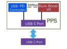 . Intersil: Inside a new architecture for USB Type-C applications
. Plastic optical fibre for battery management systems in 48 V powertrain architectures
. Losses grow at supercapacitor maker Maxwell . Power trends: Dialog enters the GaN market . New efficiency record for a large silicon solar cellPOWER TECHNOLOGIES TO WATCH
. Phase change graphene system harvests thermal energy from day/night cycle . Reinventing the magnesium battery . Report flags cybersecurity risks of renewable energy technologiesNEW POWER PRODUCTS
. IEC power entry modules now meet IEC IEC62368-1 for Audio/Video equipment . Supervisory circuit monitors system voltage with programmable delay . IGBT modules with integrated shunts reduce system costsTECHNICAL PAPERS
. Achieving Lowest Power consumption on system level: the RTC module enables it . Intersil: Inside a new architecture for USB Type-C applications. Plastic optical fibre for battery management systems in 48 V powertrain architectures
Serial CPCI module with quad-core A72 CPU
By Nick Flaherty www.flaherty.co.uk
MEN Mikro Elektronik is luanching an ARM-based CPU module in a CompactPCI Serial form-factor for embedded designs later this month.

MEN Mikro Elektronik is luanching an ARM-based CPU module in a CompactPCI Serial form-factor for embedded designs later this month.
The G40A uses the NXP ARM quad Cortex A72 LS1046A CPU with NXP data processing accelerators, fast PCI Express 3.0, USB 3.0, SATA Gen. 3 interfaces, Ethernet interfaces on front and an integrated Ethernet switch.

The G40A is a high-performance and low-power multicore CPU platform based on an ARM Cortex A72 processor with 15 year support. Being full-virtualization ready, it was designed for communication-intensive applications in harsh environments, which need high data bandwidth and computing performance, such as data collection applications onboard trains, in industrial or heavy-vehicle applications.
The MEN proprietary board management controller (BMC) monitors the G40A optional parameters such as voltages, temperature and provides a user-configurable watchdog, making it ready for applications where functional safety is required.
The memory configuration of the module includes a fast DDR4 DRAM with ECC soldered to the board to guarantee optimum shock and vibration resistance. A non-volatile SRAM, an eMMC NAND Flash device and a microSD card can also be assembled offering space for user applications or usable as a local boot medium.
The G40A is prepared for use in harsh environments with a tailored heat sink, and all components are soldered for protection against shock and vibration and it is also coated for use in humid and dusty environments.
Sunday, February 18, 2018
Google buys Xively IoT network for $50m
By Nick Flaherty www.flaherty.co.uk
Google is to acquire IoT network Xively, a division of remote management technology developer LogMeIn, for $50m.
By 2020, Gartner estimates that over 20bn connected devices will come online, and analytics and data storage in the cloud are now the cornerstone of any successful IoT solution. This acquisition, subject to closing conditions, will be added to Google Cloud's effort to provide a fully managed IoT service that easily and securely connects, manages, and ingests data from globally dispersed devices.
Related stories:
Google is to acquire IoT network Xively, a division of remote management technology developer LogMeIn, for $50m.
By 2020, Gartner estimates that over 20bn connected devices will come online, and analytics and data storage in the cloud are now the cornerstone of any successful IoT solution. This acquisition, subject to closing conditions, will be added to Google Cloud's effort to provide a fully managed IoT service that easily and securely connects, manages, and ingests data from globally dispersed devices.
Through the acquisition, Cloud IoT Core will gain deep IoT technology and engineering expertise, including Xively’s advanced device management, messaging, and dashboard capabilities. Google customers can benefit from Xively’s flexible device management platform, paired with the security and scale of Google Cloud for data analytics and machine learning.
Saturday, February 17, 2018
First Bluetooth Mesh device taps Cypress chip
By Nick Flaherty www.flaherty.co.uk

Previously, users needed to be in the immediate vicinity of a Bluetooth device to control it without an added hub. With Bluetooth mesh networking technology, the devices within the network can communicate with each other to easily provide coverage throughout even the largest homes, allowing users to conveniently control all of the devices via apps on their smartphones and tablets.
“People have become dependent on their mobile devices as integral components of their lifestyles, and they expect to extend this rich user experience in the home through the ability to directly control their connected devices using smartphones,” said Brian Bedrosian, vice president of marketing for the IoT Business Unit at Cypress . “Cypress’ Bluetooth mesh solutions enable this user experience while meeting the rigorous reliability, security and robustness required for a seamless connected media and automation environment. Our wireless solutions also deliver industry-leading coexistence and radio performance, which is essential for uninterrupted connectivity in increasingly crowded home networks. We are excited to see the adoption of Bluetooth mesh in the smart home starting with the debut of the market’s first certified consumer lighting products enabled by our technology.”
Market research firm ABI Research forecasts there will be more than 57 million Bluetooth smart lightbulbs by 2021.
Cypress’ CYW20719, CYW20706, and CYW20735 Bluetooth and Bluetooth Low Energy (BLE) combo solutions and CYW43569 and CYW43570 Wi-Fi and Bluetooth combo chips offer fully compliant Bluetooth mesh capability. Cypress also offers Bluetooth mesh certified modules and an evaluation kit. The solutions share a common, widely-deployed Bluetooth stack and are supported in version 6.1 of Cypress’ all-inclusive WICED SDK, which streamlines the integration of wireless technologies for developers of smart home lighting and appliances, as well as healthcare applications.
LEDvance, the smart bulb spin-off from Osram, has launched the market’s first Bluetooth mesh qualified LED lighting products using chip technology from Cypress Semiconductor.
Three Cypress wireless combo chips and the latest version of its Wireless Internet Connectivity for Embedded Devices (WICED ) software development kit (SDK) support the first consumer demonstration of mesh Bluetooth connectivity in the Sylvania Smart+ LED bulbs. Osram spun off LEDvance to a Chinese consortium in 2017.
Previously, users needed to be in the immediate vicinity of a Bluetooth device to control it without an added hub. With Bluetooth mesh networking technology, the devices within the network can communicate with each other to easily provide coverage throughout even the largest homes, allowing users to conveniently control all of the devices via apps on their smartphones and tablets.
“People have become dependent on their mobile devices as integral components of their lifestyles, and they expect to extend this rich user experience in the home through the ability to directly control their connected devices using smartphones,” said Brian Bedrosian, vice president of marketing for the IoT Business Unit at Cypress . “Cypress’ Bluetooth mesh solutions enable this user experience while meeting the rigorous reliability, security and robustness required for a seamless connected media and automation environment. Our wireless solutions also deliver industry-leading coexistence and radio performance, which is essential for uninterrupted connectivity in increasingly crowded home networks. We are excited to see the adoption of Bluetooth mesh in the smart home starting with the debut of the market’s first certified consumer lighting products enabled by our technology.”
Market research firm ABI Research forecasts there will be more than 57 million Bluetooth smart lightbulbs by 2021.
Cypress’ CYW20719, CYW20706, and CYW20735 Bluetooth and Bluetooth Low Energy (BLE) combo solutions and CYW43569 and CYW43570 Wi-Fi and Bluetooth combo chips offer fully compliant Bluetooth mesh capability. Cypress also offers Bluetooth mesh certified modules and an evaluation kit. The solutions share a common, widely-deployed Bluetooth stack and are supported in version 6.1 of Cypress’ all-inclusive WICED SDK, which streamlines the integration of wireless technologies for developers of smart home lighting and appliances, as well as healthcare applications.
The WICED Studio IoT development platform includes an SDK with the industry’s most broadly deployed and rigorously tested Wi-Fi and Bluetooth protocol stacks, as well as simplified application programming interfaces that free developers from needing to learn complex wireless technologies. It enables cloud connectivity in minutes with its robust libraries that uniquely integrate popular cloud services such as Amazon Web Services, IBM Bluemix, Alibaba Cloud, and Microsoft Azure, along with services from private cloud partners. WICED also supports iCloud remote access for Wi-Fi-based accessories that support Apple HomeKit which enables hub-independent platforms that connect directly to Siri voice control and the Apple Home app remotely.
Related stories:
- Bluetooth mesh kit cuts IoT developer time by six months
- Self-powered Bluetooth mesh opens up smart applications
- SiLabs mesh networking module simplifies Thread and ZigBee IoT connectivity
- Synapse and Silicon Labs Launch Wireless Module for Mesh Networks (2010)
- Broadcom looks to mesh WiFi supplier AirTies
- Bluetooth 5 chip adds mesh, Thread and Zigbee support
Subscribe to:
Posts (Atom)