All the latest quantum computer articles

See the latest stories on quantum computing from eeNews Europe

Thursday, June 28, 2018

Tensilica Fusion F1 DSP used for low power NB-IoT modem single chip

By Nick Flaherty www.flaherty.co.uk


Rafael Micro is using the Tensilica Fusion F1 configurable DSP core for its RT580 narrowband (NB) internet of things (IoT) modem IC, which integrates RF radio and includes necessary firmware support. 

The Fusion F1 DSP from Cadence Design Systems allowed Rafael Micro to implement its modem with 36 percent lower power and 45 percent smaller code size compared to a competitive processor they also evaluated. In addition, the Fusion F1 DSP’s flexible architecture makes it easier to update and upgrade to meet future NB-IoT standards.

The Fusion F1 DSP is optimised with specialist instructions for running NB wireless communications standards typically associated with IoT device communications, including protocols such as Bluetooth Low Energy, Thread and Zigbee using IEEE 802.15.4, SmartGrid 802.15.4g, Wi-Fi 802.11n and 802.11ah, 2G and LTE Category 0 release 12, 13 and 14, and global navigation satellite systems. 

“Rafael Micro’s IoT connectivity business unit focuses on developing modem radio ICs and IP for Bluetooth 5.0 Low Energy, Sub G (ISM band) and NB-IoT. In order to be competitive in the NB-IoT market, we carefully evaluated the most suitable processing engine for use in our new RT580 modem,” said Ted Sun, CEO of Rafael Micro. “Cadence’s Fusion F1 DSP met our specific requirements for minimum code size under lower operating frequency.”

“Rafael Micro’s RT580 modem will deliver customers the low cost and long battery life demanded by cellular IoT applications,” said Gerard Andrews, product marketing director for Tensilica products at Cadence. “By leveraging the efficient architecture of the Fusion F1 DSP, Rafael Micro can deliver a very flexible solution adaptable to evolving standards while maintaining the very low power consumption required by IoT applications.”

Based on the highly configurable Xtensa processor architecture, the Fusion F1 DSP offers low-energy, high-performance control and signal processing for a variety of IoT and wearable applications, including software-based GPS. 

Wednesday, June 27, 2018

A deeper dive in the ARM Cortex-M23 for secure IoT nodes

By Nick Flaherty www.flaherty.co.uk

The ARM Cortex-M23 is the smallest and most energy efficient processor with TrustZone technology. Based on the ARMv8-M baseline architecture, Cortex-M23 is aimed at constrained embedded applications where efficient security is a key requirement.

While you might think that moving TrustZone into hardware was a popular step, it has taken a while for M23 devices to reach the market. The first cores from NuMicro were launched in March 2017, but it has taken until now for the mainstream suppliers to deliver silicon.

The first of these is Microchip with the SAM architecture it inherited from its acquisition of Atmel. The SAM L10 and L11 both use the M23 core, but only the L11 implements TrustZone. Microchip has added chip-level tamper resistance, secure boot and secure key storage which, when combined with TrustZone technology, provides an hardware root of trust. It also includes an on-board cryptographic module supporting Advanced Encryption Standard (AES), Galois Counter Mode (GCM) and Secure Hash Algorithm (SHA).

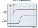
When benchmarked for power consumption, the SAM L10 received a ULPMark score of 405, which is twice that of the nearest competitor certified by the Embedded Microprocessor Benchmark Consortium (EEMBC), with the L11 just behind at a ULPMark of 400. Microchip uses proprietary picoPower technology to provide industry-leading low power consumption in active and all sleep modes.

We would expect NXP and STMicroelectronics to be launching similar M23-based chip later this year and we'll keep you updated.

Microchip has partnered with Trustonic, a member of Microchip’s Security Design Partner Programme, to offer a comprehensive security solution framework that simplifies implementation of security and enables customers to introduce end products faster. Microchip is also working with Secure Thingz and Data I/O Corporation to offer secure provisioning services for SAM L11 customers that have a proven security framework.

TrustZone for ARMv8-M brings hardware-enforced separation between the trusted and non-trusted software on each Cortex-M23 based device. As such, TrustZone provides a foundation for building embedded applications that, in the past, might have required two separate physical processors to create physical separation between the trusted and the non-trusted sides. A single Cortex-M23 processor can provide a robust solution for security requirements such as device identification management, high-value firmware protection, software certification, and secure boot, just to name a few.

The Cortex-M23 processor with TrustZone has two security states: The secure state  can access both Secure and Non-Secure resources (memories, peripherals, etc) while the Non-Secure state can only access Non-Secure resources, of course.

Code execution transitions and data accesses in the two security states is policed by hardware, minimizing switching overhead and guaranteeing determinism, which is a hallmark for all Cortex-M processors. 

Compact two-stage pipelined processor
Cortex-M23 is a simple two-stage pipelined Von Neumann processor, yet it supports the full ARMv8-M baseline instruction set.  Users familiar with the Cortex-M0+ will quickly recognize many similar features in the Cortex-M23 that bring extreme energy efficiency to these processors: WFI (Wait for Interrupts)/WFE (Wait for Event) and sleep/deep-sleep modes, sleep-on-exit, SysTick timer and optional single cycle IO.
The instruction set comprises around 80 Thumb instructions, most of which are 16-bit wide to maximize code compactness, but also include a few 32-bit instructions where efficiency gains can be made. All ARMv6-M instructions are supported to ensure ease of code migration from the Cortex-M0 and Cortex-M0+ processors. Several new instructions have been included in the ARMv8-M baseline instruction set to improve performance efficiency for conditional operations, mutually exclusive accesses, hardware divide operations, and immediate moves.
Enhanced debug and trace
An efficient and secure 32-bit processor alone does not make for successful field deployment.  Software development costs often far surpass fabrication and hardware IP costs.  The Cortex-M23 makes it easier to develop and debug software by introducing more configurable hardware breakpoints and data watch points compared to other ARMv6-M processors.  An optional Embedded Trace Macrocell (ETM) has also been added, in addition to the optional Micro Trace Buffer (MTB) which is also available as in Cortex-M0+ processor. These options give designers the choice of a more full-featured instruction trace functionality or a more cost-effective, trimmed-down, instruction trace capability.
Memory Protection Unit for task isolation
A new programmer-friendly Memory Protection Unit (MPU) based on the latest PMSAv8 architecture has been added to the Cortex-M23 processor as an option.  It can “protect” up to 16 regions for each of the Secure and Non-Secure states. Each region has a base address, ending address, access permission and memory attribute settings. In multi-tasking environments, the OS can reprogram the MPU during task context switching to define the memory permissions for each task. For example, application tasks may be granted access to all or some application data and specific peripherals. The MPU dramatically improves system reliability by protecting all other data from corruption and other peripherals from unauthorized accesses.
Easier to set up memory regions
Cortex-M23’s memory protection architecture adopts base and limit-style comparator for defining memory regions, as opposed to the previous power-of-two size, sized-aligned scheme. This improvement simplifies software development, and in some cases, reduces memory wastage when region sizes do not fit a perfect power-of-two size.
New ARMv8-M baseline instructions
New instructions have been added to enhance the Cortex-M23's capability compared to ARMv6-M implementations, but without compromising the energy efficiency. Most of these 'new' instructions (except for the security extension ones) are inherited from the ARMv7-M architecture instruction set in order to extend Cortex-M23's capability compared to the Cortex-M0+.
TrustZone for ARMv8-M brings additional instructions to the baseline instruction set. This includes the secure gateway (SG), non-secure branch (BXNS, BLXNS), and test target (TT) instructions.
Execute-only code generation
Support for the execute-only memory regions has been improved by the addition of immediate-move instructions (MOV/MOVT inherited from ARMv7-M), which facilitate immediate-data generation in execute-only code. These instructions provide the ability to produce 32-bit values via two instructions without the need to perform a literal load.
Code optimization
Conditional Compare and Branch instructions (CBNZ/CBZ inherited from ARMv7-M) improve performance for many conditional control code sequences.  Immediate branch with long offset (B.W inherited from ARMv7-M) allows for direct branch to a far target address.  And hardware integer divide instructions (SDIV/UDIV inherited from ARMv7-M) reduce processing cycles for divide operations.
Exclusive access
Load and store exclusive instructions from ARMv7-M have been added to improve the architecture consistency of Cortex-M23 processor in multicore systems where semaphores between processors can be handled with the same mechanism. In addition, to provide atomic support for C11/C++11, the load-acquire and store-release instructions are included from ARMv8-A (Thumb 32 version), including exclusive access variant of those instructions.

There is already an example Cortex-M23 IoT FPGA image, which can be used on the ARM Cortex-M Prototyping System (MPS2+).  The example Cortex-M23 IoT image includes the Cortex-M23 processor, an AHB5 subsystem, memory, timers, etc. The package also includes application note AN519 and the Cortex-M23 IoT User Guide, bare metal test code, and the pack for Keil MDK. It’s available to download from the MPS2+ page.

The SAM L10 (DM320204) and SAM L11 (DM320205) Xplained Pro Evaluation Kits are available to kick-start development. All SAM L10/L11 MCUs are supported by the Atmel Studio 7 Integrated Development Environment (IDE), IAR Embedded Workbench, Arm Keil MDK as well as Atmel START, a free online tool to configure peripherals and software for accelerated development. START also supports TrustZone technology for configuring and deploying secure applications. A power debugger and data analyser tool is available to monitor and analyse power consumption in real-time and fine-tune the consumption numbers on-the-fly to meet application needs. 


Low power IoT nodes from Eta Compute and ROHM

By Nick Flaherty www.flaherty.co.uk

Eta Compute and ROHM are looking to boost the performance of sensor networks using one of the lesser known IoT protocols.

The two have teamed up to develop ultra low power sensors using the Wireless Smart Ubiquitous Network (Wi-SUN) 802.15.4g protocol. These nodes will combine ROHM’s sensor technology and Eta Compute’s low power microcontroller for smart utility networks and the IoT.

The nodes will be designed for frequent, low-latency communication that draws less than 1 μA when resting and, more importantly, only 1 mA while sensing. This enables customers to configure devices to sense frequently and still maintain a long operating life.

The EtaCore IP can reduce power consumption by 10X enabling sensor hubs to perform sensor fusion with local computing and provide real-time data from mobile and IoT enabled devices. Operating in deep subthreshold (as low as 0.25V) the IP has been used for a self timed low power ARM Cortex-M3 controller that operates from 0.25 to 1.2 volts. The result is smaller products with fewer components operating robustly at voltages as low as 0.25V (90LP process). Eliminating a clock and operating at a lower voltage delivers that lower power.

Eta Compute has additional low voltage supporting IP such as RTC, AES, and DSP as well as an analogue-to-digital converter (ADC) sensor interface that consumes less than 3uW and an efficient power management supports dynamic voltage scaling down to 0.25V with greater than 80% efficiency are both available.

“A compact, low-power sensor node is the key enabler for the deployment of billions of devices in the IoT,” said Lip Bu Tan, Chairman of Walden International and an investor in Eta Compute as well as being teh CEO of design house Cadence Design Systems. “The team at Eta Compute has a history of successful low-power computing products and has delivered a truly compelling solution for IoT.”

“Our partnership with ROHM gives our customers access to industry-leading sensor technology combined with the industry’s lowest power microprocessor technology,” said Paul Washkewicz, vice president and co-founder of Eta Compute. “By focusing on Wi-SUN compatibility, we are providing essential components for large-scale outdoor networking required for smart cities and a diverse range of applications in an intelligent loT.”

"We are pleased to collaborate with Eta Compute. ROHM has targeted the sensor business as one of our growth strategies. We offer a wide range of sensor line-ups and propose sensor solutions, combining wireless communication devices. By pooling our resources, we will provide customers with the sensor nodes they need to deploy next-generation networks across a wide range of applications,” said Satya Dixit, Sr. Director of Solutions Marketing, at ROHM Semiconductor.

Both companies are currently demonstrating an Energy Harvesting Sensor Evaluation Board using Eta Compute’s low power MCU based on its proprietary DIAL technology. In addition, Eta Compute will demonstrate ROHM’s WI-SUN module BP35C0, Pressure Sensor BM1383AGLV, Temperature Sensor BD1020HFV, and Optical Heat Rate Sensor BH1792GLC.

Tuesday, June 26, 2018

First eSIM chips certified for embedded IoT connections

By Nick Flaherty www.flaherty.co.uk

STMicroelectronics is the first embedded SIM (eSIM) manufacturer to be accredited by the GSMA for loading eSIM chips with connection credentials such as certificates and operator profiles before shipping.

The eSIMs, customized with connection credentials, enable smaller form factors, greater security, and increased flexibility. Chip-scale, permanently embedded, and electronically reprogrammable, eSIMs save space inside IoT nodes such as smart meters, remote sensors, or gateways.

The eSIMs build on existing accreditation to manufacture eSIM chips that meet the GSMA’s specifications for security and reliability by securely applying eSIM personalization data, according to the GSMA’s Secure Accreditation Scheme for UICC Production (GSMA SAS-UP).

ST can now deliver personalized eSIMs, built around the proven ST33 secure microcontroller, directly to customers’ production facilities, ready to use with no further programming required. Equipment OEMs, mobile network operators, and SIM operating-system (OS) vendors can thus enjoy greater convenience, economy, and business efficiency by streamlining the eSIM supply chain to save handling overheads and reduce time to market.

“The SAS-UP accreditation of ST’s Rousset (France) production site for the personalization of WLCSP SIMs and eSIMs is a significant move in driving widespread adoption of trusted eSIM devices by enabling consumer and IoT device manufacturers to implement eSIM in very small form factors,” confirmed Jean-Christophe Tisseuil, GSMA’s Head of SIM and eSIM. “SAS-UP is a first and essential step towards a secure and trusted eSIM market deployment.”

“The eSIM is an important technological advance that makes it possible to build the connected world of the future, safely. The GSMA’s certification scheme governing production and personalization is critical for its success,” said Marie-France Florentin, Group Vice President, General Manager, Secure Microcontroller Division, STMicroelectronics. “Now that ST is accredited to produce and personalize eSIMs before shipping, our customers can benefit from greater efficiency and security throughout the entire supply chain, with all the safeguards and assurances provided by the GSMA’s ecosystem.”


Monday, June 25, 2018

Power news this week

By Nick Flaherty www.flaherty.co.uk at eeNews Europe Power

. Why cold computing matters for the next generation of computing

. Siemens teams for African solar microgrid projects

. SEAT uses drone to monitor huge solar farm

Power Technologies to watch
. Researchers target cathode to triple capacity of lithium ion batteries


. Fool's gold gives insight into potassium and sodium batteries


. Ultra low power vision processing chip enables miniature drones

New power products
. Analog launches first PoE++ power over ethernet chipset


. High voltage amplifiers for error-sensitive industrial applications


. Fanless 160W ATX DC-DC supply has specialised heat sink for industrial and automotive designs

Technical Papers
. Linear Tech: LTC7000/-01 MOSFET Gate Drivers


. Harwin: Key Considerations When Selecting a Connector Solution


IAR launches tools for first Cortex-M23 IoT chips

By Nick Flaherty www.flaherty.co.uk

IAR Systems ins Sweden has launched a set of tools for the new SAM L10 and SAM L11 microcontroller families available from Microchip Technology.

The SAM L10 and SAM L11 families are based on the Arm Cortex-M23 core and the SAM L11 features extensive security features such as secure boot, secure key storage and an on-board cryptographic module, protecting customers’ IP and data. 

The low power consumption makes them suitable for implementing secure IoT nodes, along with an enhanced Peripheral Touch Controller (PTC) to deliver best-in-class water tolerant and noise immune, elegant touch interfaces. 

“Low power and high security are key enablers for IoT implementations,” said Rod Drake, vice president of Microchip’s MCU32 business unit. ”Together, with IAR Systems, we are providing our customers with new possibilities for planning for security from the start and ensuring that the applications provide best-in-class energy efficiency. Our new microcontrollers and tools from IAR Systems enable a myriad of automotive, appliance, medical and consumer applications.”

“By making use of our highly optimizing tools, developers can fully leverage the performance and power saving features of the SAM L10 and SAM L11 microcontrollers,” said Anders Lundgren, Product Manager, IAR Systems. “Thanks to the smart functionality and powerful debugging technology that IAR Embedded Workbench offers, they will also be able to speed up their development and bring their IoT products faster and easier to market.”

IAR is also launching the new security development environment Embedded Trust which will enable customers to integrate security into their day-to-day workflow. 

www.iar.com/arm

Related stories:

Tuesday, June 19, 2018

Embedded AI tools for Edge Processing and secure deployment

By Nick Flaherty www.flaherty.co.uk

NXP Semiconductors has launched a set of machine learning (ML) tools for its microcontrollers along with tools for securely updating devices in the field. 

The tools operate across the low-cost microcontrollers (MCUs) to the crossover i.MX RT processors and high-performance application processors. The ML environment allows designers to choose the optimum execution engine from among ARM Cortex cores to high-performance GPU/DSP (Graphics Processing Unit/Digital Signal Processor) complexes and tools for deploying machine learning models, including neural nets, on those engines.

Embedded Artificial Intelligence (AI) is quickly becoming an essential capability for edge processing, gives 'smart' devices an ability to become 'aware' of its surroundings and make decisions on the input received with little or no human intervention. 

The ML environment enables applications in vision, voice, and anomaly detections. The vision-based ML applications use cameras as inputs to the various machine learning algorithms of which neural networks are the most popular. Voice Activated Devices (VADs) are driving the need for machine learning at the edge for wake word detection, natural language processing, and for 'voice as the user-interface' applications. NXP sees ML-based anomaly detection (based on vibration/sound patterns) revolutionising Industry 4.0 by recognizing imminent failures and dramatically reducing down-times.

The ML environment includes free software that allows customers to import their own trained TensorFlow or Caffe models, convert them to optimized inference engines, and deploy them on NXP's breadth of scalable processing solutions from MCUs to highly-integrated i.MX and Layerscape processors.

“When it comes to machine learning in embedded applications, it’s all about balancing cost and the end-user experience. For example, many people are still amazed that they can deploy inference engines with sufficient performance even in our cost-effective MCUs,” said Markus Levy, head of AI technologies at NXP. “At the other end of the spectrum is our high-performance crossover and applications processors that have processing resources for fast inference and training in many of our customer's applications. As the use-cases for AI expand, we will continue to power that growth with next-generation processors that have dedicated acceleration for machine learning.”

Another critical requirement in bringing AI/ML capability to the edge is easy and secure deployment and upgrade from the cloud to embedded devices. The EdgeScale platform enables secure provisioning and management of IoT and Edge devices. EdgeScale enables an end-to-end continuous development and delivery experience by containerizing AI/ML learning and inference engines in the cloud, and securely deploying the containers to edge devices automatically.
Members of the ecosystem include Au-Zone Technologies and Pilot.AI. Au-Zone Technologies provides the industry’s first end-to-end embedded ML toolkit and RunTime inference engine, DeepView, which enables developers to deploy and profile CNNs on NXP’s entire SoC portfolio that includes heterogeneous mixture of Arm Cortex-A, Cortex-M cores, and GPU’s. Pilot.AI has built a framework to enable a variety of perception tasks - including detection, classification, tracking, and identification - across a variety of customer platforms, ranging from microcontrollers to GPUs, along with data collection/annotation tools and pre-trained models to enable drop-in model deployment.

Monday, June 18, 2018

NXP develops first ARM R52 real time microcontroller

By Nick Flaherty www.flaherty.co.uk

NXP Semiconductors has developed a family of high-performance safe microprocessors to control vehicle dynamics in next-generation electric and autonomous vehicles based around the ARM Coretex R52 core that includes four separate processing paths for redundancy and safety. 

The new NXP S32S microprocessors will manage the systems that accelerate, brake and steer vehicles safely, whether under the direct control of a driver or an autonomous vehicle’s control.

“We see that the shift to next-generation autonomous and electric vehicles is introducing huge challenges to carmakers,” said Ian Riches, executive director in the Strategy Analytics Global Automotive Practice. “Not least of these is the ability to get silicon in hand fast enough and with enough performance headroom to ease the transitions to autonomous and advanced HEV/EV. A car can be extremely intelligent, but if it can’t act safely on a decision, you don’t have a reliable autonomous system at all.”

At 800MHz the first of the new S32 product lines, the S32S microprocessors offer the highest performance ASIL D capability available today.

The NXP S32S processors use an array of the new Arm Cortex-R52 cores, which integrate the highest level of safety features of any Arm processor. The array offers four fully independent ASIL D capable processing paths to support parallel safe computing. In addition, the S32S architecture supports a new “fail availability” capability allowing the device to continue to operate after detecting and isolating a failure – a critical capability for future autonomous applications.

Hypervisor

NXP has worked with OpenSynergy to develop a fully featured, real-time hypervisor supporting the S32S products. OpenSynergy’s COQOS Micro SDK is one of the first hypervisor platforms that takes advantage of the Arm Cortex-R52’s special hardware features. It enables the integration of multiple real-time operating systems onto microcontrollers requiring high levels of safety (up to ISO26262 ASIL D). Multiple vendor independent OS/stacks can also run on a single microcontroller. COQOS Micro SDK provides secure, safe and fast context switching ahead of today’s software-only solutions in traditional microcontrollers.

A companion ASIL D safety system basis chip, the FS66 functionally safe multi-output power supply IC, is also available, along with integrated flash memory up to 64Mbytes supporting on-the-fly, over-the-air update capability with zero processor downtime. A user programmable hardware security engine with private and public key support and a version is available with a PCIe interface for ADAS domain supervisory applications.

“When we started the development of the S32S it was clear that just building another incremental microcontroller was not what customers needed to handle the safety and performance requirements of next-generation and autonomous vehicles,” said Ray Cornyn, vice president of Vehicle Dynamics and Safety. “Our new safety processors leverage the high performance multi-core benefits of the S32 Arm platform while still supporting traditional microcontroller ease of use and environmental robustness.”

S32S will be sampling in Q4 2018 to NXP’s Automotive Alpha customers.


Power news this week

By Nick Flaherty at EENews Europe Power www.flaherty.co.uk

. IQE sees approval for LG plant refit

. Ilika leads on key UK fast charging solid state battery project

. Powerbox launches supercapacitor technology

Power technologies to watch
. Researchers target cathode to triple capacity of lithium ion batteries


. Composite carbon anode triples battery capacity


. Perovskite silicon tandem solar cell claims record efficiency


New power products
. Nexans branches out from cables with EV charger


. CAN-based 85V and 120V lithium battery chargers target industrial applications


Technical Papers
. Mentor Graphics: 8 checks for PCB design electrical sign-off


. Infineon: Deep learning neural networks demand sophisticated power


. Harwin: Key Considerations When Selecting a Connector Solution

Friday, June 15, 2018

Surveillance system connects to smartphones without compromising privacy - video

By Nick Flaherty www.flaherty.co.uk

Researchers at Purdue University in the US have found a way for public surveillance cameras to send personalised messages to people without knowing who they are.

The real-time end-to-end system called PHADE allows 'private human addressing' that doesn't use the destination's IP or MAC address. Instead it uses motion patterns as the address code for communication so that a smartphone then locally make its own decisions on whether to accept a message. The technology will be discussed at a conference in Signapore in October and the researchers see it as a direct competitor to Bluetooth beacons.

The PHADE system works using a server to receive video streams from cameras to track people. The camera builds a packet by linking a message to the address code and broadcasts the packet. Upon receiving the packet, a mobile device of each of the targets uses sensors to extract its owner's behavior and follow the same transformation to derive a second address code. If the second address code matches with the address code in the message, the mobile device automatically delivers the message to its owner.


"Our technology enables public cameras to send customized messages to targets without any prior registration," said He Wang, an assistant professor in the Purdue Department of Computer Science, who created the technology along with his PhD student, Siyuan Cao. "Our system serves as a bridge to connect surveillance cameras and people and protects targets' privacy."

PHADE protects privacy in two ways - it keeps the users' personal sensing data within their smartphones and it transforms the raw features of the data to blur partial details. The creators named the system PHADE because the blurring process "fades" people's motion details out.

PHADE can be used in places such as a museum, where visitors can receive messages with information about the exhibits they are viewing. The technology also could be implemented in shopping centres to provide consumers with digital product information or coupons.

"PHADE may also be used by government agencies to enhance public safety," said Cao. "For example, the government can deploy cameras in high-crime or high-accident areas and warn specific users about potential threats, such as suspicious followers."

Wang said surveillance camera and security companies would also be able to embed the technology into their products directly as a key feature. He also said this technology has advantages over Bluetooth-based beacons, which have difficulties in adjusting for ranges of transmission and do not allow for context-aware messaging.

Transceiver boost for steerable 5G links at 28GHz

By Nick Flaherty www.flaherty.co.uk

Scientists at Tokyo Institute of Technology have built a 28GHz transceiver that can be used for stable high-speed 5G communications with a new type of beam steering.

Most state-of-the-art transceivers designed for 5G use RF phase shifters. Accurate phase shifting is important because it allows the transceiver to guide the main lobe of the radiation pattern of the antenna array and so "point" the antenna array in a specific direction to maximise the link budget. 
Instead, the team from the Tokyo Institute of Technology, led by Associate Professor Kenichi Okada, developed a 28GHz transceiver employing a local oscillator (LO) phase shifting approach. Rather than using multiple RF phase shifters, the transceiver shifts the phase of a local oscillator in steps of 0.04° with minimal error. This allows for a beam-steering resolution of 0.1°, which is up to ten times btter than previous designs, allowing a higher throughput.

This LO phase shifting approach solves another problem of using multiple RF phase shifters: calibration complexity. RF phase shifters require precise and complex calibration so that their gain remains invariant during phase tuning, which is a very important requirement for the correct operation of the device. The situation becomes worse as the array increases in size. On the other hand, the proposed phase shifting approach results in a gain variation that is very close to zero over the entire 360° range.

The transceiver was implemented in a circuit board measuring only 4 mm × 3 mm using minimal components and provided a data rate they achieved was approximately 10 Gb/s higher than that achieved with other methods, while maintaining a phase error and gain variations an order of magnitude lower.

The results of this study are being presented at the 2018 IEEE Radio Frequency Integrated Circuits Symposium in the RMo2A session. The proposed LO phase shifting approach will hopefully help to bring forth the much-anticipated deployment of 5G mobile networks and the development of more reliable and speedy wireless communications.

Tokyo Institute of Technology - 東京工業大学

Related stories:

First standard for post-quantum signatures

By Nick Flaherty www.flaherty.co.uk

Having encryption technology that is not vulnerable to cracking by quantum computers is a major focus for security systems across the Internet, and using signatures is a key approach (see links below on our coverage).

A joint research team from the Technical University (TU) Darmstadt and the German IT security company genoa has now published an Internet standard (RFC 8391) for a quantum computer-resistant signature process.

This is the first universally recognized and usable digital signature process that can withstand the computational power of quantum computers. With digital signatures, the authenticity of sent e-mails, SSL certificates or software updates is guaranteed and these create a basis of trust for communication in the Internet of Things (IoT). The publication of the signature process as an Internet standard is a milestone for so-called post-quantum cryptography. genua is already using the process to guarantee the authenticity of software updates sent to customers.

The core of the solution is a hash-based method: Hashes work in principle only in one direction - once it encoded content can not be resolved in plain text. Because of their properties, cryptographically secure hash functions are considered to be resistant to quantum computer attacks. The research project was funded by the German Research Foundation (DFG) and the Bavarian Ministry of Economic Affairs.
Wirking with the Eindhoven University of Technology, the team submitted a draft Internet standard (RFC). These have been reviewed by the international organization IRTF (Internet Research Task Force) and are now published as RFC 8391. 

"The RFC 8391 is the first published standard on post-quantum signatures, and the research team at the TU Darmstadt and genoa has solved a problem of post-quantum cryptography, which some large corporations and organizations are working with, and is an important contributor to the Future security on the Internet, "said Matthias Ochs, CEO of genua.

genua has also launched a new research project to solve another problem in post-quantum cryptography: Securing encrypted data transmission via VPN (Virtual Private Network) via public networks such as the Internet against the foreseeable quantum leap in computing power.

More details of RFC8391 are at https://tools.ietf.org/html/rfc8391

Related stories:

Thursday, June 14, 2018

Renesas adds multirate control to multicore development tool

By Nick Flaherty www.flaherty.co.uk

Renesas has updated its RH850 multicore model-based development environment to support multirate control (multiple control periods), which is now common in systems such as engine and body control systems in automotive designs and industrial systems. 

This model-based development environment has become practical even in software development scenarios for multicore MCUs, and can reduce the increasingly complex software development burdens especially in control system development of self-driving cars.

Renesas’ earlier RH850 environment automatically allocated software to the multiple cores and although verifying performance was possible, in complex systems that included multirate control, it was necessary to implement everything manually, including the RTOS and device drivers. 

Now, to meet the ever-increasing requirements for engine and vehicle performance, and at the same time shorten product development time, by making this development environment support multirate control, it is possible to directly generate the multicore software code from the multirate control model. 

This has made it possible to evaluate the execution performance in simulation. Not only does this allow execution performance to be estimated from the earliest stages of software development, this also makes it easy to feed back the verification results into the model itself. This enables the completeness of the system development to be improved early on in the process, and the burden of developing the ever-larger scale, and increasingly complex, software systems can be significantly reduced. 

"Model-based development is becoming increasingly common, and Renesas has now completed an environment that covers from control design through automatic code generation. At the same time, since multicore software is complex, it was difficult to handle such software in earlier model-based development environments,” said Hiroyuki Kondo, Vice President of Shared R&D Division 1, Automotive Solution Business Unit at Renesas Electronics. “We were able to start working on practical application of this technology early on, and thus succeeded in creating this update. I am confident that our model-based development environment will bring dramatically improved efficiency in software development for multicore microcontrollers."

Control function development requires multirate control, such as intake/exhaust period in engine control, the period of fuel injection and ignition, and the period with which the car's status is verified. These are all different periods. By applying the technology that generates RH850 multicore code from the Simulink control mode to multirate control, it has become possible to directly generate multicore code, even from models that include multiple periods, such as engine control. Renesas also provides as an option for the Integrated Development Environment CS+ for the RH850, a cycle precision simulator that can measure time with a precision on par with that of actual systems. By using this option, it is possible to estimate the execution performance of a model of the multicore MCU at the early stages of software development. This can significantly reduce the software development period.

This conforms to the de-facto standard JMAAB control modeling guidelines for automotive model-based development. The JMAAB (Japan MBD Automotive Advisory Board), an organization that promotes model-based development for automotive control systems, recommends several control models from the JMAAB Control Modeling Guidelines. Of those, Renesas is providing in this update the Simulink Scheduler Block, which conforms to type (alpha) which provides a scheduler layer in the upper layer. This makes it possible to follow the multirate single-task method without an OS, express the core specifications and synchronization in the Simulink® model, and automatically generate multicore code for the RH850 to implement deterministic operations.

By supporting multirate control, making it easier to operate small-scale systems with different control periods with a multicore microcontroller, it is now possible to verify the operation of a whole ECU that integrates multiple systems.

The update will ship in the second half of the year. This will support Renesas’ RH850/P1H-C MCU that includes two cores initially, and also support for the RH850/E2x Series of MCUs that include up to six cores is in the planning. 

Renesas also plans to deploy this development environment to the entire Renesas autonomy Platform, including the "R-Car" Family of SoCs and plans to apply the model-based design expertise fostered in its automotive development efforts in the continually growing RX Family in the industrial area which is seeing continued increases in both complexity and scale.

Wednesday, June 13, 2018

ARM buys Stream Technologies on its way to a trillion IoT devices

By Nick Flaherty www.flaherty.co.uk

ARM doesn't buy companies very often, so its deals are a key indicator for its technology roadmap, and the latest deal combines well with the mbed embedded operating system.
Arm’s vision of a trillion connected devices by 2035 is driven by many factors, including the opportunity of IoT data. It has bought Stream Technologies to combine with mbed for the next generation embedded IoT platform.

Stream supports the physical connectivity across all major wireless protocols – such as cellular, LoRa, Satellite, etc. – that can be managed through a single user interface. Seamlessly connecting all IoT devices is important in ensuring their data is accessible at the appropriate time and cost across any use case and this capability will be integrated into the mbed platform to enable connectivity management of every device regardless of location or network. 

Founded in 2000, Stream is a leading connectivity management technology provider which maintains more than 770,000 managed subscribers and 2TB average traffic per day. Stream provides companies with a build once, deploy anywhere supply chain where any IoT device can be deployed, find a network, self-authenticate, automatically provision and connect to the lowest cost channel, removing the need to interface with multiple systems and develop several business contracts. This helps organizations reduce the time, complexity and costs of connecting devices and contributing meaningful data streams they can use.


The combination of Stream’s technology with the Mbed IoT Device Management Platform will provide a robust end-to-end IoT platform for managing, connecting, provisioning and updating devices that is easily scalable and flexible. This scalability is critical for moving from billions to trillions of connected devices. In addition, Stream will work seamlessly with GSMA compliant Embedded Subscriber Identity Module (eSIM) solutions, including Arm Kigen and other SIM solutions, to ensure secure identity and optimal connectivity for IoT devices from the chip to the cloud.

Customers will see a number of key benefits from the Stream acquisition and integration with mbed, including:
  • Single pane of glass that provides customer visibility and management capabilities throughout the device’s lifecycle – deployment, connectivity, provisioning, management, and updates
  • eSIM orchestration that communicates and connects policies enabling zero touch onboarding that drive efficiencies and scale of IoT connections
  • Global aggregation across network types and flexible wireless connectivity options that can be optimized across devices, regions, and use cases that are deployed
  • Simplified billing and reconciliation through APIs and automated controls that can charge based on any event for increased flexibility
  • Connect and manage any device regardless of network type to steer reliable and trusted data, seamlessly push new updates and features, and optimize quality-of-service and latency for troubleshooting
Mbed IoT Device Management Platform


Friday, June 08, 2018

Kerlink teams with Microshare for IoT GDPR support in the Google cloud

By Nick Flaherty www.flaherty.co.uk

LoRaWAN provides long distance low power IoT connectivity, but unlike other proprietary links the cloud integration can be lacking. The recent GDPR regulations in Europe also require that data is held securely across the entire IoT chain.

To address this, Kerlink and Microshare have developed the first seamless integration of carrier-grade LoRaWAN solutions into Google Cloud’s IoT architecture.


This ensures security of data flowing from LoRaWAN devices to extended IoT networks. As device-generated data is securely transported, annotated and unpacked in LoRaWAN networks to create context and actionable business insights, ownership rights and origins will be stamped and respected. That means network owners will be compliant with regulatory requirements, such as GDPR, the EU regulation that took effect on May 25. Most important, Microshare’s governance, audit and micro-contracting features means users can share data among ecosystem partners securely to produce efficiencies, insights and new revenue streams.

Google Cloud joined the LoRa Alliance as a Sponsor Member at the end of May, enabling Kerlink and Microshare, both active alliance members with a partnership built around LoRaWAN IoT development, to use Google Cloud.

“By integrating Microshare and Kerlink’s technologies in Google Cloud, we can create carrier-grade solutions at cloud-scale in hours rather than months,” said Yannick Delibie, Kerlink CTIO and CEO of the company’s U.S. subsidiary, Kerlink Inc. “Reducing the burden of security, scale and reliability allows both solution providers and customers to focus on rapidly delivering valuable business insights with their LoRaWAN networks.”

“We’ve seen rapid adoption of LoRaWAN as a leading enabler for easily deploying cost-effective IoT sensors globally, and we view Google’s decision to join the alliance as a validation of everything Microshare has been pursuing for the past three years,” said Ron Rock, CEO Microshare. “A lot has been achieved in making reliable, long-battery-life devices and carrier-grade networks, but this means nothing if the data generated and transported is not easily accessible to business users and securely shared between multiple organizations.”

Related stories:

Thursday, June 07, 2018

PICMG branches out with IIoT proposal, yes really

By Nick Flaherty www.flaherty.co.uk

PICMG, perhaps more well known for the AdvancedTCA, CompactPCI and COM Express hardware standards, is looking at a new specification for the Indusitrial Internet of Things (IIoT).

It has been giving live demonstrations connecting sensor and controller endpoints using new Internet of Things (IoT) methodologies at the Sensors Expo show in the US this week.

The demos are using the RESTful API "put, get, delete" commands for the connected sensor/controller interaction and PICMG has a working agreement with the DMTF (Distributed Management Task Force) to use the well-known Redfish APIs.

The new PICMG specification will intend to develop a meta-data model that encompasses a breadth of individual data models to help legacy sensors and PLCs become IoT-enabled.

www.picmg.org