Ships Cyclone IV GX Transceiver Starter Kit
Altera Corporation has stared production shipments of its Cyclone IV FPGAs, providing roughly 20,000 gates (6K logic blocks) for as little as $3 in volume, or 50,000 gates (15K logic blocks) with built in transceivers for $6.
The Cyclone IV FPGAs are designed for cost-sensitive, small form-factor applications in the wireless, wireline, broadcast, industrial and consumer markets. These devices have a combination of low cost, 25 percent lower power compared to the previous generation of Cyclone products, and high functionality that addresses high-volume, low-cost serial protocol solution needs.
"By offering Cyclone IV GX FPGAs in production shipments up to six months earlier than competing products, our customers can realize the cost, power and unique board space benefits of these devices," said Luanne Schirrmeister, senior director of component marketing at Altera. "Also, the availability of our Starter Kit gives designers confidence knowing that Cyclone IV GX devices have proven to be interoperable with other PCI Express chip sets."
Customers can begin prototyping with the Cyclone IV GX Transceiver Starter Kit which features an EP4CGX15 FPGA with approximately 15K logic elements, 540 Kbits of RAM and two integrated 2.5Gbit/s transceivers. This lowest cost transceiver starter kit priced at $395 includes all the hardware, software, design examples and documentation necessary to easily develop an FPGA design for cost-sensitive applications. This kit also allows designers to measure the FPGA's low power consumption, test
the signal quality of the FPGA transceivers, and develop and test PCI Express 1.0 endpoint designs by using Altera's PCI Express hard intellectual property (IP). In addition, the kit can be used with the Quartus(r) II Web Edition design software where no license is required.
The smallest Cyclone IV devices, the EP4CE6 and the EP4CGX15, will start as low as $3 and $6 respectively for 250K unit quantities.
Million meter contract for smart meters with British Gas
Smart meters are starting to roll out commercially in the UK with a million meter deal between Landis+Gyr, the world's largest electricity metering and smart meter supplier, and Centrica subsidiary British Gas.
The deal will see British Gas deploy up to one million of Landis+Gyr's "dual fuel" electricity and gas smart meters, along with Landis+Gyr's innovative touch screen in-home display, in UK customer homes, marking one of the largest and most advanced smart meter deployments in Europe.
Under the deployment, which will precede the UK's main smart metering rollout, consumers will be able to independently manage their energy consumption, cut their energy bills and protect the environment.
As part of the development, Landis+Gyr will share details of its smart metering system with third parties, allowing UK businesses a fast track to the creation of new and innovative solutions aimed at consumers, suppliers and utilities alike. This move - another industry first - is intended to provide other utilities with an open, practical blueprint for commercial-scale smart metering, crystallising guidance provided by both the UK Department of Energy & Climate Change (DECC) and UK regulator Ofgem (the Office of the Gas and Electricity Markets).
"Our partnership with British Gas represents a major breakthrough for smart metering in the UK. Together, we will pioneer the technical and practical standards that we hope will see every home and business in the country switch to smart metering within the next decade," said Cameron O'Reilly, CEO of Landis+Gyr.
British Gas is the first of the country's "Big Six" utilities to undertake a major deployment following the publication last December of the DECC's final plans for a national roll-out by 2020.
"We view this smart metering roll-out as one of our largest and most important projects ever," said Petter Allison, Director for Smart Metering for British Gas. "Smart meters have a fundamental role to play as they help customers become far more aware of the amount and cost of energy they use which encourages people to reduce their usage and save money."
In the UK, Landis+Gyr employs just under 500 people at manufacturing and R&D sites in Stockport and Peterborough, developing gas and electricity smart metering solutions to serve the entire Europe, Middle East and Africa (EMEA) market for the company. Landis+Gyr's technology currently supports 3 out of 4 of the UK's official Government smart meter trials.
"The UK can lead the world into second-generation smart metering and energy management and this announcement marks the beginning of that process," added Steve Cunningham, Landis+Gyr CEO for UK & Ireland. "British Gas customers will be able to actively manage their energy consumption and drive down their bills whilst a future large-scale smart grid infrastructure will allow British Gas to manage demand, protect the distribution network and optimise energy generation, including intermittent sources of renewable energy."
By combining a new generation of piezoelectric nanogenerators with two types of nanowire sensors, researchers at teh Georgia Institute of Technology have created what are believed to be the first self-powered nanometer-scale sensing devices that draw power from the conversion of mechanical energy.
The new devices can measure the pH of liquids or detect the presence of ultraviolet light using electrical current produced from mechanical energy in the environment.
Based on arrays containing as many as 20,000 zinc oxide nanowires in each nanogenerator, the devices can produce up to 1.2 volts of output voltage, and are fabricated with a chemical process designed to facilitate low-cost manufacture on flexible substrates. Tests done with nearly one thousand nanogenerators – which have no mechanical moving parts – showed that they can be operated over time without loss of generating capacity.
It has been developed to monitor the eyes of patients with glaucoma, but the latest technology from STMicroelectronics for a Swiss medical startup points the way to integrating a display in a contact lens.
ST is to develop and supply a wirelessMEMS sensor that acts as a transducer, antenna and mechanical support for additional read-out electronics in a system developed by Sensimed in Geneva. This solution will enable better management of glaucoma patients via earlier diagnosis and treatment that is optimally tailored to the individual patient.
Sensimed's Triggerfish is based on a “smart” contact lens that uses a tiny embedded strain gauge to monitor the curvature of the eye over a period of, typically, 24 hours, providing valuable disease management data that is not currently obtainable using conventional ophthalmic equipment.
Sensimed’s ingenious solution is a two-part system comprising the smart contact lens and a small receiver worn around the patient’s neck. In addition to the strain gauge the lens contains an antenna, a tiny dedicated processing circuit and an RF transmitter to communicate the measurements to the receiver. The lens is powered via the received radio waves and does not need to be connected to a battery. The embedded components are positioned in the lens in such a way that they do not interfere with the patient’s vision. The lens is fitted by the ophthalmologist and when the patient returns the next day the ophthalmologist removes the lens and receiver, obtaining a complete record of IOP changes over the preceding 24 hours.
“Application trials are confirming the significant benefits that our unique platform can provide and the next step is to commercialize the product to a larger number of centers in selected geographies,” said Jean-Marc Wismer, CEO of Sensimed. “
ST expects the development of the MEMS sensor to be completed in Q2 2010 and manufacturing to start in Q3 2010, with availability outside trials to doctors and patients subject to regulatory approvals. Sensimed and ST anticipate progressively rolling out the product country-by-country across Europebeginning in Q3and entering the US market by the end of 2011.
“We have a strong focus on developing and manufacturing wireless sensor networks for diagnostics and other applications in medicine. This wireless, self-powered, on-body sensor will be used in a product that promises to greatly help the millions of people at risk and suffering from glaucoma,” said Benedetto Vigna, General Manager of STMicroelectronics’ MEMS, Sensors and High Performance Analog division. “Sensimed’s imaginative application perfectly illustrates how, by working with healthcare experts, we can combine two different disciplines and know-how, along with our manufacturing infrastructure, to improve the health and wellbeing of people all over the world.”
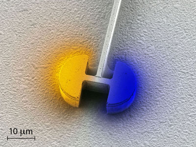
The laser is 30 micrometers long, eight micrometers high and has a wavelength of 200 micrometers. This makes the laser considerably smaller than the wavelength of the light it emits – difficult, as lasers normally can’t be smaller than their wavelength! So instead of using a resonant cavity, the researchers used an electrical resonant circuit made up of an inductor and two capacitors where the light is effectively “captured” in it and induced into self-sustaining electromagnetic oscillations on the spot using an optical amplifier.
This means the size of the resonator is no longer limited by the wavelength of the light and can in principle be scaled down to any size. This makes the microlaser very interesting for chip manufacturers as an optic alternative to the transistors. “If we manage to approximate the transistors in terms of size using the microlasers, one day they could be used to build electro-optic chips with an extremely high concentration of electronic and optic components”, says researcher Christoph Walther.
Skinput is a method that allows the body to be appropriated for finger input using a novel, non-invasive, wearable bio-acoustic sensor, to be presented in April.
Devices with significant computational power and capabilities can now be easily carried on our bodies. However, their small size typically leads to limited interaction space (e.g., diminutive screens, buttons, and jog wheels) and consequently diminishes their usability and functionality. Since we cannot simply make buttons and screens larger without losing the primary benefit of small size, we consider alternative approaches that enhance interactions with small mobile systems.
One option is to opportunistically appropriate surface area from the environment for interactive purposes. For example, Scratch Input is technique that allows a small mobile device to turn tables on which it rests into a gestural finger input canvas. However, tables are not always present, and in a mobile context, users are unlikely to want to carry appropriated surfaces with them (at this point, one might as well just have a larger device). However, there is one surface that has been previous overlooked as an input canvas, and one that happens to always travel with us: our skin.
Appropriating the human body as an input device is appealing not only because we have roughly two square meters of external surface area, but also because much of it is easily accessible by our hands (e.g., arms, upper legs, torso). Furthermore, proprioception (our sense of how our body is configured in three-dimensional space) allows us to accurately interact with our bodies in an eyes-free manner. For example, we can readily flick each of our fingers, touch the tip of our nose, and clap our hands together without visual assistance. Few external input devices can claim this accurate, eyes-free input characteristic and provide such a large interaction area.
Fortune magazine has listed its most admired companies in the world, with a separate break-out for semiconductor companies.
Among semiconductor companies evaluated, STMicroelectronics is ranked the 6th most admired, in its first year as a participant in the survey. Additionally, it is the highest-ranking Europe-based chipmaker on the list.
The “World’s Most Admired Companies” survey debuted in the U.S. in 1983 and began ranking companies worldwide in 1997. Companies are rated by their peers based on nine factors including quality of products or services, quality of management, global competitiveness, and soundness of financial position to name a few. This year approximately 4,170 top executives, directors, and financial analysts assessed companies in their own industries, and voted on companies being considered for the overall most admired list. A total of 667 companies from 33 countries across 55 industries were surveyed.
General Motors R&D and several universities are working on a system that would use data gathered from an array of vehicle sensors and cameras and project images generated by compact ultra violet lasers directly onto the entire surface of the windshield. Head up displays are already used in cars for data suuch as speed, but this aims to use the whole windscreen for an augmenteed reality system.
“We’re looking to create enhanced vision systems,” says Thomas Seder, group lab manager-GM R&D. His team is working with Carnegie Mellon University and The University of Southern California, as well as other institutions, to create a full windshield head-up system leveraging night vision, navigation and camera-based sensor technologies to improve driver visibility and object detection ability.
“Let’s say you’re driving in fog, we could use the vehicle’s infrared cameras to identify where the edge of the road is and the lasers could ‘paint’ the edge of the road onto the windshield so the driver knows where the edge of the road is,” said Seder.
Enhanced vision systems are a 21st Century take on Head up display technology that GM was the first to market in 1988. Designed to help keep driver attention on the road ahead by displaying important information such as vehicle speed, lane change indicator status and vehicle warning messages directly into the driver’s field of vision, head-up display systems are currently available on the GMC Acadia, Chevrolet Corvette, Buick LaCrosse and Cadillac STS.
Scientists and lab technicians at GM’s global research and development in Warren, MI, are now developing next-generation head-up systems that could transform the everyday windshield into a device that can make driving even safer. While the full windshield head-up system has not yet been identified for a future GM vehicle program, Seder says some of the supporting technologies could end up in GM vehicles in the near-term future.
Coated with a series of transparent phosphors which emit visible light when excited by a light beam—in this case from a compact laser—the windshield becomes a large area transparent display, instead of current HUD systems that use only a small portion of the windshield.
The ability to use such an expansive surface enables the system to alert drivers of potential dangers that may exist outside of the normal field of vision—including children playing or motorcycles passing.
On that foggy day, maybe worsened by sleet or snow, the enhanced vision system could combine night vision with the head-up system to identify and highlight the precise location of animals roaming along the side of the road that could have avoided recognition with the naked eye.
“This design is superior to traditional head down display-based night vision systems, which require a user to read information from a traditional display, create a mental model and imagine the threat’s precise location in space,” Seder said
As an added safety feature, the head-up system can be combined with automated sign reading technology, similar to the Opel Eye system that debuted on the 2009 Opel Insignia, to alert the driver if they are driving over the posted speed limit or if there’s impending construction or other potential problems ahead. Additionally, the system can use navigation system data to alert the driver of their desired exit by reading overhead traffic signs.
“We have done testing on a number of drivers and their performance is better relative to head-down systems that are commonly used in vehicles today,” Seder said. “It’s a compelling design.”
Among electronic equipment OEMs, spending in 2010 will rise to $177.9 billion, up 13 percent from $157.0 billion in 2009. iSuppli forecasts that the total spend by EMS providers in 2010 will amount to $37.7 billion, up 15.1 percent from $32.8 billion in 2009.The rise in spending among OEMs assumes the inclusion of all chips consumed by end products regardless of how the chips are purchased—including OEM direct purchases as well as procurement conducted through EMS or distributors.
OEMs jockey for top spot in semiconductor spending
“The increase in OEM semiconductor spending in 2010 represents a turnaround for the market from 2009,” said Min-Sun Moon, senior analyst for semiconductor spend and design at iSuppli. “Spending last year plunged by 16.1 percent—due not only to a decline in the average selling price of chips but also because of a drop in shipments. Although still cautious, electronic OEMs this year are gearing up to gain more share in their respective markets—a strategy that will translate into greater semiconductor spending.”
Hewlett-Packard in the lead
Hewlett-Packard is projected to be the top OEM semiconductor spender in 2010, a position it will retain after taking the No.-1 spot away from Nokia, which fell to third place in 2009. HP will spend an estimated $12.6 billion this year, compared to $10.99 billion in 2009.
In second place among top OEM spenders for 2010 will be Samsung Electronics, expected to spend $12.5 billion, compared to $10.3 billion last year. Notwithstanding its runner-up ranking for two consecutive years, Samsung is projected to take over the No.-1 title in 2011, thanks to its broad range of businesses—including new wireless handsets, thin LED-backlit TVs and 3-D TVs—that will drive increased semiconductor spend for the company.
Following Nokia in third place, Apple will become the fourth largest spender in 2010, moving past Dell. Though not even appearing in the ranks of the Top-10 semiconductor purchasers before 2006, Apple started advancing after introducing the iPhone in 2007 and is expected to surpass Nokia to land at No. 3 in 2011.
The attached figure presents the world’s Top-20 OEMs ranked by semiconductor spending in 2010.
EMS on the rise
Among EMS providers, the projected rise in spending this year follows a significant drop in revenue for the group in 2009 due to big declines in OEM shipment orders. However, large providers can expect to recover quickly in 2010. The top EMS spenders in 2010 will include Foxconn, Flextronics, Jabil Circuit and Celestica.
For No.-1 Foxconn, spending will reach $22.6 billion in 2010, up 18.7 percent from $19.0 billion in 2009, boosted by the company’s manufacturing of HP products, Nintendo’s Wii, Sony’s PlayStation 3 and Apple’s iPod, iPhone and the soon-to-be-released iPad.
Following Foxconn in second place will be Flextronics, projected to spend $7 billion in 2010, up 8.8 percent from $6.4 billion last year. The EMS giant, headquartered in Singapore and whose clients include Sony Ericsson, HP and Research In Motion, will continue to expand manufacturing facilities in China.
The biggest markets for EMS providers include compute platforms and wireless communications. However, the share of smaller markets will increase over time, indicating that OEMs will start outsourcing other types of products besides computers and handsets.
Mentor Graphics is teaming up with STMicroelectronics on a broad collaboration to develop advanced design solutions at 32nm and down to 20nm.
The three-year joint-development project, named DeCADE, seeks to build on advanced design solutions for SoC (System On Chip) development for Digital and Analog design, including system-level approaches, design methodologies, place and route strategies, optical correction for advanced manufacturing, modeling, electrical characterization and parasitic extraction. ST will significantly contribute to the development of these new SoC design tools, which will give ST a head start in its ability to deliver customer-focused semiconductor chips and platforms. DeCADE will provide design solutions for core CMOS technologies as well as for value-added and application-specific derivative technologies that are developed from the core CMOS process. These projects can make a fundamental difference in chip capability and, performance, as well as in system-solution cost; among the value-added derivative technologies being considered by the DeCADE projects include RF (Radio Frequency) and wireless technologies, as well as 3D Packaging and chip stacking technologies. As a recognized pioneer in these technologies, ST’s participation will assure the strength of the design solutions’ foundation and ensure that its next-generation tools contribute to its maintaining product and technology leadership.
"This joint development effort will provide ST with tools to develop state-of-the-art Systems-on-Chips (SoCs) at 32-nm and below for ST's customers, taking full advantage of the strong Silicon Process, Device Modeling and Design know-how present on the Crolles Site," said Philippe Magarshack, STMicroelectronics General Manager of Central CAD & Design Solutions. "This ST-Mentor Graphics joint effort further reinforces the Crolles cooperative R&D cluster, which already gathers partners that develop and enable low-power SoCs and value-added application-specific technologies and is a great example of a project developed within the framework of the Nano2012 program." This is a strategic R&D program, led by ST, which gathers research institutes and industrial partners and is supported by French national, regional and local authorities. The program aims to create one of the world's most advanced R&D clusters for the development of new generations of semiconductor technology platforms at the nano-electronic level “As a leading provider of semiconductor based solutions, ST is an excellent partner with whom to explore and develop the design methodologies that the market will need over the next decade," said Greg Hinckley, President of Mentor Graphics. “We look forward to this collaboration as a further extension of Mentor Graphics efforts with our long term customer ST.”
Store For TVs, Blu-ray Players, and Home Theatre Systems linking to WiFi phones
Following the success of applications stores on mobile phones - particularly with Apple and Android - the next move is to apps running on Android on consumer equipment, and Samsung Electronics in the US is the first to officially launch its own site.
Samsung Apps is the first HDTV-based application store where users can download applications from select 2010 Samsung HDTVs, Blu-ray Players and Home Theatre systems via the upgraded Internet@TV – Content Service. Samsung Apps provides consumers with an expanded, easy to navigate selection of content and applications from leading services like The Associated Press, Netflix, Pandora, Twitter, USA TODAY, and VUDU. More than 20 apps will be available by the end of March, with hundreds expected by the end of the year. The new application platform allows content owners and developers to develop apps that work across multiple devices for the ease and convenience of consumers.
Applications can be downloaded and viewed all while watching TV and premium apps will be available for purchase via the platform’s transactional interface in the second half of 2010. “We are making a significant step forward in delivering a more personalized, navigable and easy to use connected TV experience,” said John Revie, senior vice president of home entertainment for Samsung Electronics America. “Samsung Apps will be offered in numerous TV models as well as across our Blu-ray Players and Home Theater Systems, so consumers can conveniently access a variety of content through many forms that fit their needs.”
The apps span information, video, lifestyle, games, and sports from trackin news to renting movies. Additionally, several apps in 2010 will allow interactivity between HDTVs and select Samsung WiFi-enabled phones. Consumers, for example, will be able to play Texas hold ’em poker with friends, where the TV screen shows the table and the phone serves as the controller, while showing cards in your hand like a real poker game. Developer Opportunity
Content and application developers will have new opportunities to build applications, content and services through the Samsung Apps Software Developers Kit (SDK). The forthcoming developers program will be an open platform that encourages anyone from premium content owners to individual developers, to create their own applications. Samsung expects many additional partners to become Samsung App developers by the end of 2010.
2010 Consumer Electronics Outlook up on 2009, 2008
Despite a 5% decline from 2008 to 2009, IMS Research sees relatively strong growth in smartphones, portable media players, set-top boxes, LCD televisions and refrigeration appliances for 2010, which are expected to significantly contribute to global CE revenues of $406 billion during the year. Global revenues for consumer electronics reached $375 billion (excluding home office equipment and low-end mobile phones) in 2009. Combined revenues for years 2010 to 2012 are forecast to pass $1.3 trillion.
"In addition to typical CE devices such as TV sets, set-top boxes, digital cameras, smartphones and netbooks, we are expecting to see increased revenue for the CE industry in major home appliances and telehealth, not to mention the nascent connected tablet market," said Shane Walker, IMS Research’s Consumer Electronics Group Manager. "Contributions to the 2010 Yearbook from our Power & Energy and InMedica research groups show that refrigeration units and room air-conditioners will account for 60% of major home appliance revenue and 19% of overall CE revenue. While telehealth remains an emerging category for CE, consumer-led telehealth services could prove to be the disruptive influence required for professional care authorities to drive telehealth forward”.
The new study, The Consumer Electronics Yearbook – 2010 edition, provides detailed market analysis on 40 product types covering portable consumer devices, active speaker systems, PMP docking stations, digital picture frames, home theater systems, televisions, appliances and home medical equipment. It offers a concise and unique perspective on the consumer electronics industry through both quantitative and qualitative analysis compiled from several studies recently produced by IMS Research.
A few additional key findings from the study include:
After replacement rates for digital cameras fell by 5% in 2009, revenues are forecast to increase in 2011 and 2012 on growth in shipment volumes. Revenues will begin to decline slightly starting in 2013 as average prices continue to drop.
Portable navigation device sales are forecast to grow in India and South America as improvements in accurate up-to-date mapping increase.
Households displaying Internet video on the TV set via a game console, proprietary device, or a Blu-ray player comprised the vast majority of total Internet TV households in 2008 and 2009.
HD 1-Way set-top boxes experienced a temporary spike in shipments as a result of the US NTIA Set-top Box subsidy. After 2009, IMS Research expects HD 1-Way boxes to hold steady at 6-7% of total shipments.
Cisco Joins Panasonic & Samsung to Accelerate Consumer Adoption
The most advanced millimetre wave startup, SiBEAM, has raised $36.5m in its D round of funding to accelerate the consumer adoption of its 60GHz short range wireless technology.
All of SiBEAM’s original investors contributed to this round including U.S. Ventures Partners (USVP) and New Enterprise Associates (NEA), joined by new partners in SiBEAM’s success, Lux Capital and Hatteras Funds. Best Buy and Cisco have also contributed strategic equity investments to support SiBEAM’s growth as well as fund future projects for personal computing and mobile devices.
"SiBEAM continues to deliver on its promise to bring high-quality, lossless wireless high definition capabilities to the A/V home entertainment market. Their team has executed well on its plans and has brought in nearly all leading CE manufacturers as customers through its work with the growing WirelessHD Consortium,” said Adam Grosser, General Partner at Foundation Capital which led the round. “This market adoption further supports our confidence in SiBEAM’s technology and the team’s capabilities to drive and solidify the company’s leadership in the exciting and high-growth wireless connectivity market.”
SiBEAM’s second generation 60GHz chipset with its OmniLink60 Technology was brought into mass production earlier this year for A/V receivers, home theater-in-a-box systems, Blu-ray players, set-top boxes, media center PCs, and consumer laptops.
“This round of financing is a significant milestone for SiBEAM as it demonstrates the continued growth of our business and potential for significant investment return even in a challenging economy. With these funds, we can grow our business toward profitability in the burgeoning wireless A/V market,” said John LeMoncheck, President and CEO of SiBEAM. “SiBEAM continues to receive extensive interest from CE and PC manufacturers worldwide that are eager to integrate simple, cost effective and high quality wireless streaming capability into their products.”
Open standard 3D API specification available immediately Provides performance, quality and flexibility enhancements including tessellation and double precision shaders Tight integration with OpenCL for seamless visual computing
The next generation of 3D API (application programming interface) that is deployed on all major desktop operating systems has been launched, along with a retrofit to allow the new capabilities on existing graphics processors. OpenGL is vital for desktop systems but also for smartphones with the OpenES standard and WebGL as an API for better Web graphics.
The OpenGL 4.0 specification has been defined by the OpenGL ARB (Architecture Review Board) working group at Khronos, and includes the GLSL 4.00 update to the OpenGL Shading language in order to enable developers to access the latest generation of GPU acceleration with significantly enhanced graphics quality, acceleration performance and programming flexibility. This new release continues the rapid evolution of the royalty-free OpenGL standard to enable graphics developers to portably access cutting-edge GPU functionality across diverse operating systems and platforms. The full specification is available for immediate download at http://www.opengl.org/registry .
OpenGL 4.0 further improves the close interoperability with OpenCL™ for accelerating computationally intensive visual applications. OpenGL 4.0 also continues support for both the Core and Compatibility profiles first introduced with OpenGL 3.2, enabling developers to use a streamlined API or retain backwards compatibility for existing OpenGL code, depending on their market needs.
OpenGL 4.0 has been specifically designed to bring significant benefits to application developers, including:
two new shader stages that enable the GPU to offload geometry tessellation from the CPU;
per-sample fragment shaders and programmable fragment shader input positions for increased rendering quality and anti-aliasing flexibility;
drawing of data generated by OpenGL, or external APIs such as OpenCL, without CPU intervention;
shader subroutines for significantly increased programming flexibility;
separation of texture state and texture data through the addition of a new object type called sampler objects;
64-bit double precision floating point shader operations and inputs/outputs for increased rendering accuracy and quality;
performance improvements, including instanced geometry shaders, instanced arrays, and a new timer query.
Lastly, Khronos has simultaneously released an OpenGL 3.3 specification, together with a set of ARB extensions, to enable as much OpenGL 4.0 functionality as possible on previous generation GPU hardware; providing maximum flexibility and platform coverage for application developers. The full OpenGL 3.3 specification is also available for immediate download at http://www.opengl.org/registry
“The release of OpenGL 4.0 is a major step forward in bringing state-of-the-art functionality to cross-platform graphics acceleration, and strengthens OpenGL’s leadership position as the epicenter of 3D graphics on the web, on mobile devices as well as on the desktop,” said Barthold Lichtenbelt, OpenGL ARB working group chair and senior manager Core OpenGL at NVIDIA. “NVIDIA is pleased to announce that its upcoming Fermi-based graphics accelerators will fully support OpenGL 4.0 at launch.”
“AMD sees the release of OpenGL 4.0 as another major accomplishment for the OpenGL ARB,” said Ben Bar-Haim, vice president of design engineering at AMD. “AMD contributes to the Khronos workgroups, and we consistently find that Khronos is successful at developing healthy, thriving, and evolving open standards such as OpenGL and OpenCL.”
“OpenGL 4.0 continues the ARB’s schedule-driven roll-out of new functionality, and this significant major release enables developers to access leading-edge GPU functionality across multiple platforms with full backwards compatibility,” said Neil Trevett, president of the Khronos Group and vice president at NVIDIA. “OpenGL continues to be a keystone in the Khronos API ecosystem, through driving innovation into OpenGL ES and WebGL to bring high-performance programmable graphics to mobile platforms and the Web, and by interoperating with OpenCL to create a seamless visual and compute platform for application developers.”
GE Intelligent Platforms has launched a rugged 6U OpenVPX Single Board Computer (SBC) that is the first with an integrated GPGPU (general purpose computing on a graphics processing unit) capability. The IPN250 delivers high levels of computing performance for size, weight and power (SWaP) constrained platforms at lower cost, creating new application opportunities. It enables system integrators to deploy a single COTS module where previously multiple disparate modules would have been required – undertaking, for example, front end processing of sensor-acquired data, digital signal processing, backend processing and graphics/video processing, and delivering high resolution mission critical data more rapidly than has previously been possible.
The IPN250 is the second product from GE to feature NVIDIA’s CUDA technology: the CUDA-enabled GRA111 3U graphics board was announced in November 2009. CUDA is becoming increasingly attractive to systems integrators in military and aerospace since it has been demonstrated to be capable of enabling performance gains of up to 100x in a range of applications: its innovative technology and openness create the opportunity for improved productivity and sustainable competitive advantage. It is increasingly mandated by some Department of Defense (DoD) program offices because it offers increased flexibility and reduced cost of ownership when compared with previous FPGA-centric solutions.
“The IPN250 allows customers to easily deploy sophisticated applications developed on NVIDIA-enabled PCs directly onto a rugged GPGPU platform, reducing risk to schedules and shortening time to deployment,” said Peter Cavill, General Manager, Military & Aerospace Products at GE Intelligent Platforms. “It reduces cost by leveraging the growing ecosystem of software programmers creating high performance computing applications in standard development environments such as CUDA, OpenCL, OpenGL and MATLAB, to support long term code portability across multiple generations of COTS hardware platforms.”
The IPN250 combines NVIDIA’s latest GT240 96-core GPU with an Intel® Core™2 Duo processor operating at 2.26GHz and 8 GBytes of DDR3 SDRAM to deliver up to 390 GFLOPS of performance per card slot, depending on the application. It is designed from the ground up to be compliant with the OpenVPX standard, ensuring interoperability with a broad range of other OpenVPX boards. Providing a computationally-dense platform, the IPN250 is ideal for demanding applications that are constrained in terms of size, weight and power (SWaP). It is also VITA48/REDI-compliant, allowing it to be deployed in the harshest environments: build options for air-, spray- and conduction cooling are available.
The IPN250 feature set includes two primary data plane, 10 Gigabit Ethernet ports supporting multi-board switched fabric OpenVPX architectures. A 16-lane PCI Express gen2 interface on the P2 expansion plane provides high speed interconnect for multi-board GPGPU clusters as well as system I/O to PCI Express-enabled sensor modules such as GE’s family of Xilinx Virtex5 and Virtex6 mezzanine cards. Two 1000Base-T and two 1000Base-Bx control plane ports are available, together with additional PCI Express, USB 2.0 , SATA, COM ports, GPIO , audio and TV input. Video and multimedia is supported via the dual link DVI, HDMI and VGA ports directly into the NVIDIA GT240 device to cater for a wide range of interfaces.
GE Intelligent Platforms’ AXISLib advanced multiprocessor software development VSIPL, DSP and math libraries for CUDA and INTEL SSE4 facilitate application development and code portability for the IPN250 and future GPGPU platforms. In addition to NVIDIA’s CUDA environment, supported software includes Linux, Windows, Microsoft DirectX, OpenCL, OpenGL and MATLAB, together with NVIDIA’s PureVideo Technology and PhysX.
Britain should invoke some of the spirit of Inmos – a government-owned semiconductor company set up more than 30 years ago – to establish a £300m series of new technology centres to lay the basis for economic growth, according to a top government adviser.
IBM scientists have unveiled a significant step towards replacing electrical signals that communicate via copper wires between computer chips with tiny silicon circuits that communicate using pulses of light. As reported in the recent issue of the scientific journal Nature, this is an important advancement in changing the way computer chips talk to each other.
The device, called a nanophotonic avalanche photodetector, is the fastest of its kind and could enable breakthroughs in energy-efficient optical computing.
The IBM device uses the “avalanche effect” in Germanium, a material currently used in production of microprocessor chips. Conventional avalanche photodetectors are not able to detect fast optical signals because the avalanche builds slowly.
“This invention brings the vision of on-chip optical interconnections much closer to reality,” said Dr. T.C. Chen, vice president, Science and Technology, IBM Research. “With optical communications embedded into the processor chips, the prospect of building power-efficient computer systems with performance at the Exaflop level might not be a very distant future.”
The avalanche photodetector demonstrated by IBM is the world’s fastest device of its kind. It can receive optical information signals at 40Gbps (billion bits per second) and simultaneously multiply them tenfold. Moreover, the device operates with just a 1.5V voltage supply, 20 times smaller than previous demonstrations. Thus many of these tiny communication devices could potentially be powered by just a small AA-size battery, while traditional avalanche photodetectors require 20-30V power supplies.
“This dramatic improvement in performance is the result of manipulating the optical and electrical properties at the scale of just a few tens of atoms to achieve performance well beyond accepted boundaries,” said Dr. Assefa, the lead author on the paper. “These tiny devices are capable of detecting very weak pulses of light and amplifying them with unprecedented bandwidth and minimal addition of unwanted noise.”
In IBM’s device, the avalanche multiplication takes place within just a few tens of nanometers (one-thousandths of a millimeter) and that happens very fast. The tiny size also means that multiplication noise is suppressed by 50% - 70% with respect to conventional avalanche photodetectors. The IBM device is made of Silicon and Germanium, the materials already widely used in production of microprocessor chips. Moreover it is made with standard processes used in chip manufacturing. Thus, thousands of these devices can be built side-by-side with silicon transistors for high-bandwidth on-chip optical communications.
The Avalanche Photodetector achievement, which is the last in a series of prior reports from IBM Research, is the last piece of the puzzle that completes the development of the “nanophotonics toolbox” of devices necessary to build the on-chip interconnects.
In December 2006, IBM scientists demonstrated silicon nanophotonic delay line that was used to buffer over a byte of information encoded in optical pulses - a requirement for building optical buffers for on-chip optical communications.
In December 2007, IBM scientists announced the development of an ultra-compact silicon electro-optic modulator, which converts electrical signals into the light pulses, a prerequisite for enabling on-chip optical communications.
In March 2008, IBM scientists announced the world’s tiniest nanophotonic switch for “directing traffic” in on-chip optical communications, ensuring that optical messages can be efficiently routed .
The report of this work, entitled “Reinventing Germanium Avalanche Photodetector for Nanophotonic On-chip Optical Interconnects,” by Solomon Assefa, Fengnian Xia, and Yurii Vlasov of IBM’s T.J. Watson Research Center in Yorktown Heights, N.Y. is published in the March 2010 issue of the scientific journal Nature.
IBM has a long history of pioneering advanced silicon technologies to help enhance performance, while reducing size and power consumption. Such advances include the development of the world’s first copper-based microprocessor; silicon-on-insulator (SOI), a technology that reduces power consumption and increases performance by helping insulate the millions of transistors on a chip; and strained silicon, a technology that “stretches” material inside the silicon decreasing the resistance and speeding the flow of electrons through transistors.
INMC to Offer UK SMEs Opportunities to Network at Key International Events
The Nanotechnology Knowledge Transfer Network (NanoKTN), one of the UK’s primary knowledge-based networks for Micro and Nanotechnologies, and the Institute of Nanotechnology (IoN), a professional membership organisation for the nanotechnology industry, has announced a collaboration to encourage and support global business development for UK SMEs.
The partnership will see the launch of the International NanoMicroClub (INMC) and the opportunity for selected SMEs to host workshops at three major international events, offering vital networking opportunities.
If the future of UK nanotechnology is going to be securely embedded in the global market, we need to ensure UK SMEs are including international business development and collaboration in the marketing mix. However, with international marketing costing around 14 times the equivalent domestic marketing budget, it limits the international interaction that a UK SME can undertake. International business development therefore poses a significant barrier to SMEs, which this project seeks to address.
The INMC was created through a partnership between the NanoKTN and IoN and builds on the IoN’s existing NanoMicroClub. The club aims to provide a platform for UK micro and nanotechnology companies to network and engage internationally with global markets, previously inaccessible due to a lack of funding. The club will be taking UK based companies developing nanotechnologies to three well known and highly regarded international events and highlighting them to an international audience through specific and pre arranged networking and brokerage sessions.
Building on networks developed within the NanoKTN and IoN, the INMC partnering workshops will comprise short presentations from UK delegates, followed by facilitated one-on-one meetings between company principals.
“The INMC aims to help SME’s project themselves into important export markets through research, collaboration and business development. Commercial outcomes from international deals may take time but this only reinforces the need to provide support to SMEs for international business development,” said Alec Reader, Director of the NanoKTN. “This sort of framework of support in the early stages can make the difference between success and failure and is crucially important to the UK nanotechnology market.”
The three events that are planned cover the three major trading areas, USA, Europe and Japan. Each event will have a particular theme specific to the trading strength of each area. The first event in the USA will be at the NSTI conference in Anahiem, CA and will be themed around the bio-nanotechnology area. Further events in Europe and Japan are planned in the last quarter of 2010 and first quarter of 2011 respectively. Further details of these events will be available in due course.
“The NanoMicroClub has been assisting UK nanotechnology companies for over five years as it has provided a networking platform to assist companies in accessing new customers and routes to market. Our new partnership with the NanoKTN will allow us to really go global and strengthen our successful formula” said Del Stark, Business Development Manager of the Institute of Nanotechnology.

![Reblog this post [with Zemanta]](http://img.zemanta.com/reblog_e.png?x-id=5deb1dcc-023d-4d08-b407-c0b93241fb09)

![Reblog this post [with Zemanta]](http://img.zemanta.com/reblog_e.png?x-id=c8caa302-0adb-4fa4-a84c-c010eb21074c)
![Reblog this post [with Zemanta]](http://img.zemanta.com/reblog_e.png?x-id=1eb65808-f3ea-4e7e-9d77-2a30f18e1951)


![Reblog this post [with Zemanta]](http://img.zemanta.com/reblog_e.png?x-id=c6369f4e-9d46-4bb7-a97e-16ffb7be492b)
![Reblog this post [with Zemanta]](http://img.zemanta.com/reblog_e.png?x-id=fc8f0e65-15c9-498e-833e-a9454a5d75ba)

![Reblog this post [with Zemanta]](http://img.zemanta.com/reblog_e.png?x-id=e636e8bc-536a-4b84-87dc-dcebdf135a80)

![Reblog this post [with Zemanta]](http://img.zemanta.com/reblog_e.png?x-id=dee561cc-2e6f-46c5-ac2f-28fb91e15737)
![Reblog this post [with Zemanta]](http://img.zemanta.com/reblog_e.png?x-id=ffa430f5-63a1-4724-bf3f-0ba1bd900650)

![Reblog this post [with Zemanta]](http://img.zemanta.com/reblog_e.png?x-id=5fc5a550-bb09-4f07-9557-19d8ea13131e)
![Reblog this post [with Zemanta]](http://img.zemanta.com/reblog_e.png?x-id=f6ce20da-b775-401a-8536-3426a218ea30)
![Reblog this post [with Zemanta]](http://img.zemanta.com/reblog_e.png?x-id=bf1160f2-fb0a-45af-adee-b32f1a362ded)
![Reblog this post [with Zemanta]](http://img.zemanta.com/reblog_e.png?x-id=6cc4688c-5f10-4e69-afcf-bb5cd8002daf)
![Reblog this post [with Zemanta]](http://img.zemanta.com/reblog_e.png?x-id=24996df5-6482-44f1-b08d-dab138c23a11)
![Reblog this post [with Zemanta]](http://img.zemanta.com/reblog_e.png?x-id=3e8724e3-3980-4613-8ab2-ab7b06324d55)
![Reblog this post [with Zemanta]](http://img.zemanta.com/reblog_e.png?x-id=95ff1a02-5b7f-43eb-98fc-fd1c1a31c869)
![Reblog this post [with Zemanta]](http://img.zemanta.com/reblog_e.png?x-id=16752876-ca0e-4a7a-b3bd-eb37372e0fd6)
![Reblog this post [with Zemanta]](http://img.zemanta.com/reblog_e.png?x-id=f1e6964a-9602-4013-af93-f37243dd47b7)