By Nick Flaherty
www.flaherty.co.ukResearchers at EPFL in Zurich have developed a low cost transmitter for terahertz signals used for sensing.
The team at the Power and Wide-band-gap Electronics Research Laboratory (POWERlab), led by Prof. Elison Matioli, built a nanoscale device that can generate extremely high-power signals in just a few picoseconds to produces high-power THz waves.
The technology, which can be mounted on a chip or a flexible medium, could one day be installed in smartphones and other hand-held devices. THz waves are largely used for object detection through other materials.
The device generates high-intensity waves from a spark, with the voltage spiking from 10 V (or lower) to 100 V in the range of a picosecond. The device is capable of generating this spark almost continuously, meaning it can emit up to 50 million signals every second. When hooked up to antennas, the system can produce and radiate high-power THz waves.
The device consists of two metal plates situated very close together, down to 20nm apart. When a voltage is applied, electrons surge towards one of the plates, where they form a nanoplasma. Once the voltage reaches a certain threshold, the electrons are emitted almost instantly to the second plate. This rapid movement enabled by such fast switches creates a high-intensity pulse that produces high-frequency waves.
Conventional electronic devices are only capable of switching at speeds of up to one volt per picosecond. The extremely short rise times down to five picoseconds were only limited by the measurement set-up. By integrating these devices with dipole antennas, high-power terahertz signals with a power–frequency trade-off of 600 milliwatts terahertz squared were emitted, much greater than that achieved by the state of the art in compact solid-state electronics.
The new device can be more than ten times faster, can generate both high-energy and high-frequency pulses. "Normally, it's impossible to achieve high values for both variables," said Matioli. "High-frequency semiconductor devices are nanoscale in size. They can only cope with a few volts before breaking out. High-power devices, meanwhile, are too big and slow to generate terahertz waves. Our solution was to revisit the old field of plasma with state-of-the-art nanoscale fabrication techniques to propose a new device to get around those constraints."
"These nanodevices, on one side, bring an extremely high level of simplicity and low-cost, and on the other side, show an excellent performance. In addition, they can be integrated with other electronic devices such as transistor. Considering these unique properties, nanoplasma can shape a different future for the area of ultra-fast electronics", said Mohammad Samizadeh Nikoo, a PhD student at the POWERlab.
The technology could have wide-ranging applications beyond generating THz waves. The ease of integration and the compactness of the nanoplasma switches could enable their implementation in several fields, such as imaging, sensing, communications and biomedical applications.
"We're pretty sure there'll be more innovative applications to come," adds Matioli.

 . Ventilator technology takes centre stage
 . OneWeb teeters on the brink
 . Electric aircraft maker raises $240m
 . ION Energy teams for battery management in electric excavator
 . £30m for UK power technology development network
 . €11m for Munich battery digital twin startup
 . Design kit dramatically reduces PMIC power and die size
 . Titanium potassium-ion battery cathode has high potential
 . Two pin D²PAK packaging for SiC diodes
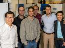 . Machine learning slashes battery fast charging scheme development time


 .
.  .
.  .
.  .
.  .
.  .
.  .
.  .
.  .
. 
