All the latest quantum computer articles

See the latest stories on quantum computing from eeNews Europe
Showing posts with label PCI Express. Show all posts

Wednesday, January 05, 2011

USB3.0 drives the 'zero client' computer with no internal processing power - CES

New Approach to Computing Powered by USB 3.0 at CES 2011
By Nick Flaherty www.flaherty.co.uk

The rise of the high speed USB3.0 technology, particularly the optical version, is leading to a renaissance in the thin client, driving the idea of the 'zero client', says VIA Labs.


The Zero Client concept is an evolution of the Thin Client computing model that takes Shared-Resource Computing to the next level with no independent hardware processing facilities. Through multiple zero clients, many users can be simultaneously connected to a single server, leveraging the abundant computing power and flexibility provided by today’s mainstream systems. In contemporary zero client implementations, the end user experience is often bandwidth dependant since each Zero Client requires video, audio, and data connections.
Before the speed and flexibility of USB 3.0, Zero Clients utilized USB 2.0 or Ethernet, and frequently offered inferior multimedia capabilities and a degraded user experience. VIA Labs is demonstrating a zero client based on the new USB 3.0 standard which offers massive bandwidth capacity with its portfolio of USB 3.0 Superspeed controllers where several client terminals can now simultaneously enjoy a full user experience including HD multimedia, using the optical version to get the distance to the terminal previously provided by Ethernet.
“The zero client concept exemplifies the benefits that higher bandwidth USB 3.0 technologies can offer,” said Gibson Chen, Vice President of Sales at VIA Labs. “USB 3.0 based zero clients can enjoy a full and immersive PC experience simultaneously across several client stations thanks to the far greater data throughput that our leading USB 3.0 controllers offer.”
VIA labs is the only company in the world to have a complete USB 3.0 solution with host, hub and device controller products that are quickly setting industry standards. With an emphasis on delivering leading bandwidth performance while also pursing aggressive power-savings, VIA Labs is paving the way forward for new applications and devices in the broader electronics industry.
Complying with USB 3.0, USB Battery Charging, and eXtensible Host Controller Interface specifications (xHCI) the VIA VL800 offers four downstream facing ports that enable the simultaneous operation of multiple peripheral devices and includes USB Battery charging support to rapidly charge smart phones, tablets, and other compatible devices.
The industry’s first USB 3.0 hub controller, the VIA VL810 is a highly integrated, single chip solution provides maximum data transfer rates of up to 5Gbps, or ten times the throughput available to USB 2.0 based devices. Enables up to four USB devices to be connected to a single downstream port of a host or hub.
The VIA VL700 USB 3.0 to SATA Controller is a highly integrated single chip solution that allows users to connect any SATA hard disk drive (HDD), solid state drive (SSD), and optical disc drive (ODD) devices to their PC over USB 3.0. Details can be found here: http://www.via-labs.com/en/products/vl700/index.jsp
The VIA VL750 USB 3.0 to NAND Flash Controller is the first of its kind in the world, featuring a 4-channel memory controller with interleaving support, the VIA VL750 offers consumers blisteringly fast data transfer speeds of 100MB/s or more on larger capacity ‘thumb’ drives and USB sticks.

Related articles
CES: USB 3.0 facing slow take-up from manufacturers (v3.co.uk)
USB 3.0: Everything You Need to Know (itexpertvoice.com)
You: Intel Confirms USB 3.0 on Chief River Notebook Platform (everythingusb.com)
USB-IF Announces Second Certified USB 3.0 Host Controller (eon.businesswire.com)
USB 3.0 Support in Windows 7 (devcurry.com)
Enhanced by Zemanta

Monday, January 03, 2011

VIA Launches Embedded Industry’s First Dedicated Graphics Card with 3D and DDR3

By Nick Flaherty www.flaherty.co.uk


VIA eH1 card offers DX10.1 graphics and multi-screen HD video content for embedded systems

 VIA Technologies has developed a graphics card designed specifically for the embedded market. The eH1 is a DX10.1 compliant, multi-display card for the PCI Express slot that comes with the three year product longevity guarantee that is vital for embedded designs and is the most power-efficient discrete graphics and video solution on the market today. The VIA eH1 AIB uses the 64bit S3 Chrome 5400E GPU graphics chip for DirectX 10.1, OpenGL 3.1, OpenGL ES 2.0  and offers multi-stream 1080p HD video decoding and Stereoscopic 3D rendering capability alongside 512Mbytes of DDR3 memory. This makes it the ideal solution for a range of embedded applications that require advanced graphics and video on multiple displays.
 “The VIA eH1 hits a real sweet spot for the embedded industry as a whole,” said Daniel Wu, Vice President, VIA Embedded Platform Division at VIA Technologies. “Offering technologies like DX10.1, OpenGL/CL, plus multi-channel HD video playback on an extremely low power AIB will excite system integrators who want to bring the latest features to existing platforms.”

VIA eH1: Embedded Graphics and Video
The VIA eH1 is a low profile PCI Express add-in-board designed for next generation embedded applications in a range of segments including digital signage and advertising, POS, POI, gaming or any embedded application where graphics and HD video is streamed on two displays.

l            PCIe 2.0 Bus Interface
l            512MB DDR3
l            Low profile form factor
l            Dual-Link DVI and HDMI (with HDCP)
l            Fully programmable DirectX 10.1 Unified Shader Core
l            OpenGL 3.1 + OpenGL ES 2.0
l            GPGPU on OpenCL 1.0
l            H.264 and VC-1 support for Blu-Ray
l            Support for resolutions up to 2560x1600
l            1080p/1080i/720p HD-decode
l            Steroscopic 3D capable
l            Dual display support

The VIA eH1 can be used in conjunction with a number of VIA EPIA board products and can supplement any existing system that uses a x1, x4, x8 or x16 PCIe slot. Samples of the VIA eH1 are available now to project customers upon request.


Details regarding the S3 Chrome 5400E can be found at S3 Graphics

Enhanced by Zemanta

Wednesday, April 28, 2010

Rugged XMC Module For Video Streaming From Unmanned Vehicles

ICS-8580 combines two TI DSP processors and Altera FPGA

GE Intelligent Platforms has launched a powerful, compact, easy to use and flexible answer to the problem of capturing, compressing and delivering video. The ICS-8580 responds to the rapid growth in unmanned vehicles and their requirement to deliver high quality mission video over links that are often bandwidth-constrained. It is designed to be a simple, plug-and-play solution that requires minimal integration or software development.
The ICS-8580’s XMC form factor means that it is small, lightweight at 100 grams/3.5 ounces and consumes little power – typically, 10 – 15 watts. These features, in conjunction with its rugged design, mean that it can be deployed in a wide range of demanding military and aerospace environments. Its flexibility is further enhanced by its ability to support numerous video formats with either two channels of high definition video or four channels of standard definition video. The ICS-8580 features the ultra-efficient, industry standard H.264 video compression codec, but is software-reconfigurable to enable it to support alternatives such as JPEG2000.
“With the ICS-8580, we have taken a task that was previously difficult, time-consuming and often costly and made it simple, quick and inexpensive,” said Christopher Lever, Global Product Manager, Sensor Processing and I/O at GE Intelligent Platforms. “For prime contractors, systems integrators and OEMs, the ICS-8580 delivers a sustainable competitive advantage through its use of innovative technologies, increasing customer productivity while minimizing program cost and risk and speeding time-to-market.”
The ICS-8580 provides input support for HD/ED/SD analog input signals, analog RGB formats from VGA to UXGA, as well as digital input formats such as 3G-SDI, DVI, and HDMI up to a maximum resolution of 1,920 x 1,080 or 1,600 x 1,200 pixels. An Altera Arria II GX FPGA combined with TI DSP signal processing provide exceptional compute power in a video XMC platform.
Two TI TMS320DM6467 DSPs provide processing capability to achieve two streams of up to 1080p H.264 (or JPEG 2000) encoding. Up to four streams of SD input data can be compressed in parallel. The encoded bitstream can be accessed via PCI Express, or output directly as Gigabit Ethernet RTP/UDP packets.
High-speed A/D devices - supporting resolutions up to 1,600 x 1,200 for graphics type inputs and 1,920 x 1,080 for HD video inputs - provide input digitization of the various supported analog video formats. The FPGA controls data capture and routing and can be used in a variety of ways, while the TI DSP co-processors provide efficient and streamlined video data processing. If required, the system can be loaded with custom FPGA and DSP code to perform a broad range of video processing functions on the video input streams.
Data input and output is available using a carrier card, PCI Express connectivity, or via rear I/O. Analog or digital input data can be supported through the rear I/O connectors. Up to 768 MB of DDR2 SDRAM is supplied on-board. The FPGA has 256 MB and each DSP device has 256 MB.
Reblog this post [with Zemanta]

Monday, April 12, 2010

Low cost PCIe development kit accelerates system design

Achieve Working PCI Express Hardware in Thirty Minutes
 

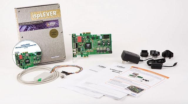
Lattice Semiconductor has developed a low cost PCI Express development kit for its LatticeECP3 family of low power FPGAs.  Based on a new ECP3 PCI Express solutions board, the kit accelerates development of PCI Express designs.  The kit has been developed from the ground up to accelerate the evaluation of PCI Express technology, demonstrate a range of solutions that match typical application requirements and speed users to design exploration. 
The new kit features four key capabilities for quick evaluation and rapid prototyping of low cost PCI Express system design.  First, the kit enables users to bring up running PCI Express hardware in thirty minutes or less.  Second, various demos included in the kit address control plane through data plane performance requirements.  Third, source files for the demos are available that enable rebuilding designs up to a known good starting point.  Finally, the kit enables a rapid transition to design exploration through the included software tools, IP enabled evaluation process and project source directories.

“The LatticeECP3 FPGA is an excellent low power, high value programmable platform for PCI Express,” said Shakeel Peera, Lattice’s Director of Strategic Marketing for High Density Solutions. “The new LatticeECP3 PCI Express development kit will help users reduce complexity and shrink the time-to-market window for their PCI Express designs.”

The kit is an all-inclusive package optimized for creating a design with the low-power, low-cost LatticeECP3 FPGA family with a highly-optimized, low-cost PCI Express evaluation board that enables both x1 and x4 endpoint evaluation and design. There are a variety of demo executables, from a basic demo for control plane applications, throughput demo for high-bandwidth applications, color bar demo and an image transfer demo - that show how to address different design performance requirements.  
The 60 day software tools license includes an x1/x4 endpoint IP core and scatter-gather DMA IP core permit users to get up and running right away and available on both Windows and Linux platforms.
The components of the LatticeECP3 PCI Express development kit have been configured to work together to enable fast system evaluation and design.  With the help of easy step-by-step instructions, designers can expect to have a demo running in as little as 30 minutes, and a design validated in less than two hours.


LatticeECP3 FPGA Family
The LatticeECP3 FPGA family is five devices that offer standards-compliant multi-protocol 3.2G SERDES, DDR1/2/3 memory interfaces and high performance, cascadable DSP slices that are ideal for high performance RF, baseband and image signal processing.  Toggling at 1Gbps, the LatticeECP3 FPGAs also feature the fastest LVDS I/O available in a mid-range FPGA family, as well as embedded memory of up to 6.8 Mbits.  Logic density varies from 17K LUTs to 149K LUTs with up to 586 user I/O.  The LatticeECP3 FPGA family is ideally suited for deployment in high volume cost- and power-sensitive wireline and wireless infrastructure applications, as well as security/surveillance, medical and industrial applications.

The development kit is available now, with a list price of $895.00.  The kit can be ordered through Lattice sales or through the Lattice on-line store at http://www.latticesemi.com/store/dev_kits.cfm.
Reblog this post [with Zemanta]

Monday, March 29, 2010

Altera Rolls Out $3 FPGAs

Ships Cyclone IV GX Transceiver Starter Kit
Altera Corporation has stared production shipments of its Cyclone IV FPGAs, providing roughly 20,000 gates (6K logic blocks) for as little as $3 in volume, or 50,000 gates (15K logic blocks) with built in transceivers for $6.
The Cyclone IV FPGAs are designed for cost-sensitive, small  form-factor applications in the wireless, wireline, broadcast, industrial and consumer markets. These devices have a combination of low cost, 25 percent lower power compared to the previous generation of Cyclone products, and high functionality that addresses high-volume, low-cost serial protocol solution needs.
"By offering Cyclone IV GX FPGAs in production shipments up to six months earlier than competing  products, our customers can realize the cost, power and unique board space benefits of these devices," said Luanne Schirrmeister, senior director of component marketing at Altera. "Also, the availability of our Starter Kit gives designers confidence knowing that Cyclone IV GX devices have proven to be interoperable with other PCI Express chip sets."
Customers can begin prototyping with the Cyclone IV GX Transceiver Starter Kit which features an EP4CGX15 FPGA with approximately 15K logic elements, 540 Kbits of RAM and two integrated 2.5Gbit/s transceivers. This lowest cost transceiver starter kit priced at $395 includes all the  hardware, software, design examples and documentation necessary to easily develop an FPGA design for cost-sensitive applications. This kit also allows designers to measure the FPGA's low power consumption, test
the signal quality of the FPGA transceivers, and develop and test PCI Express 1.0 endpoint designs by using Altera's PCI Express hard intellectual property (IP). In addition, the kit can be used with the Quartus(r) II Web Edition design software where no license is required.
The smallest Cyclone IV devices, the EP4CE6 and the EP4CGX15, will start as low as $3 and $6 respectively for 250K unit quantities.


Reblog this post [with Zemanta]