All the latest quantum computer articles

See the latest stories on quantum computing from eeNews Europe

Friday, August 24, 2018

Calibration errors in fab equipment cost chipmakers millions of dollars

By Nick Flaherty www.flaherty.co.uk

A study from the US National Institute of Standards and Technology (NIST) has uncovered a source of error in an industry-standard calibration method that could lead chip makers to lose a million dollars or more in a single wafer run.

The error occurs when measuring very small flows of exotic gas mixtures in the chemical vapour deposition (CVD) and plasma etching. The exact amount of gas injected into the chamber is critically important to these processes and is regulated by a mass flow controller (MFC).

"Flow inaccuracies cause nonuniformities in critical features in wafers, directly causing yield reduction," said Mohamed Saleem, Chief Technology Officer at Brooks Instrument, a US MFC maker. "Factoring in the cost of running cleanrooms, the loss on a batch of wafers scrapped due to flow irregularities can run around $500,000 to $1,000,000. Add to that cost the process tool downtime required for troubleshooting, and it becomes prohibitively expensive."

Modern fabs rely on accurate gas flows controlled by MFCs which as typically calibrated using the "rate of rise" (RoR) method, which makes a series of pressure and temperature measurements over time as gas fills a collection tank through the MFC.

"Concerns about the accuracy of that technique came to our attention recently when a major manufacturer of chip-fabrication equipment found that they were getting inconsistent results for flow rate from their instruments when they were calibrated on different RoR systems," said John Wright of NIST's Fluid Metrology Group which conducted the error analysis.

Wednesday, August 22, 2018

CTIA launches US cybersecurity certification programme

By Nick Flaherty www.flaherty.co.uk

CTIA, the wireless industry association, has launched a Cybersecurity Certification Programme for cellular-connected Internet of Things (IoT) devices. The program is the first of its kind to be developed in collaboration with US nationwide wireless providers.

By offering certification for IoT devices built from the ground up with cybersecurity in mind, the program will protect consumers and wireless infrastructure, while creating a more secure foundation for smart cities, connected cars, mHealth and other IoT applications.

"America's wireless industry has long been a leader in cybersecurity best practices and establishing an industry-led cybersecurity certification program for IoT devices is a major step in building a trusted, secure wireless ecosystem for the Internet of Things," said Tom Sawanobori, CTIA SVP and Chief Technology Officer. "The IoT Cybersecurity Certification Program harnesses CTIA's network of authorized labs and reflects our commitment to securing networks and devices in an increasingly connected wireless world."

Wireless operators, technology companies, security experts and test labs collaborated to develop the program's test requirements and plans. The program builds upon IoT security recommendations from the National Telecommunications and Information Administration (NTIA) and the National Institute of Standards and Technology (NIST).

"IoT security is fast becoming a priority as the global market grows to 3.5 billion cellular-connected IoT devices, with a 48 percent 5G mobile adoption rate in the U.S. by 2023, according to the latest Ericsson Mobility Report," said Tomas Ageskog, Head of Digital Services at Ericsson North America.

CTIA's Certification Working Groups have developed and managed product test plans and certification requirements for devices, networks and other wireless technologies, with over 70,000 certification requests handled to date by over 100 CTIA Authorized Test Labs. These programs ensure interoperability between wireless devices and networks, as well as set standards for a secure, high-performing and innovative wireless ecosystem.

The CTIA IoT Cybersecurity Certification Program will begin accepting devices for certification testing starting in October 2018

Tuesday, August 21, 2018

New cryptographic standards add secure access control for the IoT

By Nick Flaherty www.flaherty.co.uk

The ETSI Technical Committee on Cybersecurity has released two specifications on Attribute-Based Encryption (ABE) that describe how to protect personal data securely with fine-grained access controls that are particularly suited to the Internet of Things (IoT).

ABE is an asymmetric, multi-party cryptographic scheme that bundles access control with data encryption. In such a system, data can only be decrypted if the set of attributes of the user key matches the attributes of the encryption. For instance, access to particular data could only be granted to a specific role and a person with sufficient experience and authority. 

Because ABE enforces access control at a cryptographic (mathematical) level, it provides better security assurance than software-based solutions. It is also space-efficient, since only one ciphertext is needed to cater for all access control needs of a given data set.

Attribute-Based Encryption has been identified by ETSI as a key enabler technology for access control in highly distributed systems, such as 5G and the IoT:

ETSI TS 103 458 describes the high-level requirements for Attribute-Based Encryption. One objective is to provide user identity protection, preventing disclosure to an unauthorized entity. It defines personal data protection on IoT devices, WLAN, cloud and mobile services, where secure access to data has to be given to multiple parties, according to who that party is.

ETSI TS 103 532 specifies trust models, functions and protocols using Attribute-Based Encryption to control access to data, thus increasing data security and privacy. It provides a cryptographic layer that supports both variants of ABE- Ciphertext Policy and Key Policy - in various levels of security assurance. This flexibility in performance suits various forms of deployments, whether in the cloud, on a mobile network or in an IoT environment. The cryptographic layer is extensible and new schemes can be integrated in the standard to support future industry requirements and address data protection challenges in the post-quantum era.

Both specifications enable compliance with the General Data Protection Regulation, enforced since May 2018, by allowing secure exchange of personal data among data controllers and data processors.

A standard using Attribute-Based Encryption has several advantages for the industry. It provides an efficient, secure-by-default access control mechanism for data protection that avoids binding access to a person’s name, but instead to pseudonymous or anonymous attributes. ABE offers an interoperable, highly scalable mechanism for industrial scenarios where quick, offline access control is a must, and where operators need to access data both in a synchronous manner from the equipment as well as from a larger pool of data in the cloud.

This means ETSI TS 103 532 is particularly well-suited to the Industrial IoT as it enables access control policies to be introduced after data has been protected, it provides forward-compatibility with future business and legal requirements, such as the introduction of new stakeholders.

www.etsi.org

Related stories:

  • MISRA-compliant embedded crypto toools target IoT
  • Low cost crypto chip to secure the Internet of Things

  • Using Static Analysis to Improve IIoT Device Security
  • Maxim launches reference design for IoT node security 
  • Two factor security IP designed into IoT microcontrollers 
  • Cybersecurity researchers design a chip that checks itself 

Monday, August 20, 2018

Power News this week

By Nick Flaherty www.flaherty.co.uk at eeNews Europe

. Sila Nano raises $75m for silicon anode battery materials


. Ørsted to buy US onshore wind developer


. Deal creates global centre for electric vehicles in Germany


.


POWER TECHNOLOGIES TO WATCH


. Single-atom transistor promises lower-power electronics


. Researchers to test laser charging of UAVs in flight


NEW POWER PRODUCTS


. 3kW AC-DC power supply targets test systems


. 1A 3.2MHz regulators with LDO reduce footprint and EMI


. 1Pbyte SSD rulers slash data centre power


TECHNICAL PAPERS


. National Instruments: Hardware-in-the-Loop Testing for Power Electronics Systems

Adesto shows steps to resistive memories

By Nick Flaherty www.flaherty.co.uk

IoT chip designers Adesto Technologies is planning to show new research showing the potential for Resistive RAM (RRAM) technology in high-reliability applications such as automotive. 

Adesto Fellow Dr. John Jameson, who led the research team, will share the results at the ESSCIRC-ESSDERC 48th European Solid-State Device Research Conference, being held in Germany on September 4th, 2018.

RRAM has great potential to become a widely used, low-cost and simple embedded non-volatile memory (NVM), as it uses simple cell structures and materials which can be integrated into existing manufacturing flows with as little as one additional mask. However, many RRAM technologies to-date have faced integration and reliability challenges. 

The research at Adesto on the technology, which it calls CBRAM, shows that the devices consume less power, requires fewer processing steps, and operates at lower voltages as compared to conventional embedded flash technologies.

“We’re delighted to share our latest RRAM research with the prestigious technical community at ESSCIRC-ESSDERC,” said Dr. Venkatesh Gopinath, VP of CBRAM and RRAM Technology and Production Development at Adesto. “For the first time, RRAM is being demonstrated as an ideal low-cost, one-mask embedded NVM for high-reliability applications. Adesto was the first company to bring commercial RRAM devices to market, and now our CBRAM technology is production-proven for IoT and other ultra-low power applications. Our continued innovation and advancements will bring the benefits of CBRAM to an even broader range of applications.”

Related stories:

Thursday, August 16, 2018

Printed chipless wifi tags add everyday objects to the Internet of Things.

By Nick Flaherty www.flaherty.co.uk


PRINTED THIN, FLEXIBLE LIVETAG TAGS IN COMPARISON WITH A PIECE OF PHOTO PAPER (FAR LEFT). CREDIT: XINYU ZHANG ET AL.

Engineers at the University of California in San Diego in the US have developed printable metal tags that could be attached to everyday objects to act as smart sensors connected to the Internet of Things (IoT).

The metal tags are made from patterns of copper foil printed onto thin, flexible, paper-like substrates and are made to reflect WiFi signals. The tags work essentially like "mirrors" that reflect radio signals from a WiFi router. When a user's finger touches these mirrors, it disturbs the reflected WiFi signals in such a way that can be remotely sensed by a WiFi receiver such as a smartphone.

The tags can be tacked onto plain objects that people touch and interact with every day, like water bottles, walls or doors. These plain objects then essentially become smart, connected devices that can signal a WiFi device whenever a user interacts with them. The tags can also be fashioned into thin keypads or smart home control panels that can be used to remotely operate WiFi-connected speakers, smart lights and other Internet of Things appliances.

"Our vision is to expand the Internet of Things to go beyond just connecting smartphones, smartwatches and other high-end devices," said Xinyu Zhang, a professor of electrical and computer engineering at the UC San Diego Jacobs School of Engineering and member of the Centre for Wireless Communications at UC San Diego. "We're developing low-cost, battery-free, chipless, printable sensors that can include everyday objects as part of the Internet of Things."

Zhang's team have called the technology "LiveTag." These metal tags are designed to only reflect specific signals within in the WiFi frequency range. By changing the type of material they're made of and the pattern in which they're printed, the researchers can redesign the tags to reflect either Bluetooth, LTE or cellular signals.

The tags have no batteries, silicon chips, or any discrete electronic components, so they require hardly any maintenance--no batteries to change, no circuits to fix.

As a proof of concept, the researchers used LiveTag to create a paper-thin music player controller complete with a play/pause button, next track button and sliding bar for tuning volume. The buttons and sliding bar each consist of at least one metal tag so touching any of them sends signals to a WiFi device. The researchers have so far only tested the LiveTag music player controller to remotely trigger a WiFi receiver, but they envision that it would be able to remotely control WiFi-connected music players or speakers when attached to a wall, couch armrest, clothes, or other ordinary surface.

The researchers also adapted LiveTag as a hydration monitor. They attached it to a plastic water bottle and showed that it could be used to track a user's water intake by monitoring the water level in the bottle. The water inside affects the tag's response in the same way a finger touch would--as long as the bottle is not made of metal, which would block the signal. The tag has multiple resonators that each get detuned at a specific water level and could be used to deliver reminders to a user's smartphone to prevent dehydration.

"When patients return home, they could use this technology to provide data on their motor activity based on how they interact with everyday objects at home--whether they are opening or closing doors in a normal way, or if they are able to pick up bottles of water, for example. The amount, intensity and frequency of their activities could be logged and sent to their doctors to evaluate their recovery," said Zhang. "And this can all be done in the comfort of their own homes rather than having to keep going back to the clinic for frequent motor activity testing," he added.

Another example is tagging products at retail stores and assessing customer interest based on which products they touch. Rather than use cameras, stores could use LiveTag as an alternative that offers customers more privacy, said Zhang.

The researchers note several limitations of the technology. LiveTag currently cannot work with a WiFi receiver further than one meter (three feet) away, so researchers are working on improving the tag sensitivity and detection range. Ultimately, the team aims to develop a way to make the tags using normal paper and ink printing, which would make them cheaper to mass produce.

WiFi used to detect weapons and liquids

By Nick Flaherty www.flaherty.co.uk

Researchers at Rutgers University in the US have used standard WiFi with multiple MIMO antennas to detect metals and liquids in luggage rather than using more comlex terahertz wireless systems.

Using WiFI means the detection system is easy to set up, reduces security screening costs and avoids invading privacy such as when screeners open and inspect bags, backpacks and luggage.

“This could have a great impact in protecting the public from dangerous objects,” said Yingying (Jennifer) Chen, study co-author and a professor in the Department of Electrical and Computer Engineering in Rutgers–New Brunswick’s School of Engineering. “There’s a growing need for that now.”

The study – led by researchers at the Wireless Information Network Laboratory (WINLAB) in the School of Engineering – included engineers at Indiana University-Purdue University Indianapolis (IUPUI) and Binghamton University.

The system requires a WiFi device with two to three antennas and can be integrated into existing WiFi networks. The system analyzes what happens when wireless signals penetrate and bounce off objects and materials.

Experiments with 15 types of objects and six types of bags demonstrated detection accuracy rates of 99 percent for dangerous objects, 98 percent for metal and 95 percent for liquid. For typical backpacks, the accuracy rate exceeds 95 percent and drops to about 90 percent when objects inside bags are wrapped, said Chen.

"In large public areas, it’s hard to set up expensive screening infrastructure like what’s in airports,” Chen said. “Manpower is always needed to check bags and we wanted to develop a complementary method to try to reduce manpower.”

Next steps include trying to boost accuracy in identifying objects by imaging their shapes and estimating liquid volumes, she said.

Related stories:

Wednesday, August 15, 2018

Top ten chip mergers shows limit to deals

By Nick Flaherty www.flaherty.co.uk

The size of traditional semiconductor acquisitions may have hit a limit says Bill McClean at IC Insights. However the analysis acknowledges that it does not include more vertical integratisuch as the recent $18bn Broadcom/CA deal.
Mega-mergers become less likely because of the high-dollar value of major acquisitions, increasing scrutiny from regulators, rising protectionism among more countries, and growing global trade frictions, says the report.


The global semiconductor industry has been reshaped by a historic wave of mergers and acquisitions during the past three years, with about 100 M&A agreements being reached between 2015 and the middle of 2018 with the combined value of these transactions being more than $245 billion, based on data collected by IC Insights 

Figure 1 ranks the 10 largest semiconductor merger and acquisition announcements and underscores the growth in size of these M&A transactions. Eight of the 10 largest announcements occurred in the last three years with only the biggest deal (Qualcomm buying NXP) failing to be completed.

A record-high $107.3 billion in semiconductor acquisition agreements were announced in 2015. The second highest total for semiconductor M&A agreements was then reached in 2016 at $99.8 billion. Semiconductor acquisition announcements reached a total value of $28.3 billion in 2017, which was twice the industry’s annual average of about $12.6 billion in the first half of this decade but significantly less than 2015 and 2016, when M&A was sweeping through the chip industry at historic levels. In the first six months of 2018, semiconductor acquisition announcements had a total value of about $9.6 billion, based on IC Insights’ running tally of announced M&A deals.

The demise of Qualcomm’s pending $44 billion purchase of NXP Semiconductors in late July along with growing regulatory reviews of chip merger agreements, efforts by countries to protect domestic technology, and the escalation of global trade friction all suggest semiconductor acquisitions are hitting a ceiling in the size of the deals. It is becoming less likely that semiconductor acquisitions over $40 billion can be completed or even attempted in the current geopolitical environment and brewing battles over global trade.

IC Insights believes a combination of factors—including the growing high dollar value of major chip merger agreements, complexities in combining large businesses together, and greater scrutiny of governments protecting their domestic base of suppliers—will stifle ever-larger mega-transactions in the semiconductor industry in the foreseeable future. 

IC Insights points out that the list only covers semiconductor suppliers, chipmakers, and providers of integrated circuit intellectual property (IP) and excludes acquisitions of software and system-level businesses by IC companies such as Intel’s $15.3 billion purchase of Mobileye in August 2017. This M&A list also excludes transactions involving semiconductor capital equipment suppliers, material producers, chip packaging and testing companies, and design automation software firms.

Qualcomm’s $44 billion cash purchase of NXP would have been the largest semiconductor acquisition ever if it was completed, but the deal—originally announced in October 2016 at nearly $39 billion and raised to $44 billion in February 2018—was canceled in the last week of July because China had not cleared the transaction. China was the last country needed for an approval of the merger, and it was believed to be close to clearing the purchase in 2Q18, but growing threats of tariffs in a brewing trade war with the U.S. and moves to block Chinese acquisitions of American IC companies caused China to taken no action on the $44 billion acquisition in time for a deadline set by Qualcomm and NXP. U.S.-based Qualcomm canceled the acquisition on July 26 and quickly paid NXP in the Netherlands a $2 billion breakup fee so the two companies could move on separately.

Prior to Qualcomm’s failed $44 billion offer for NXP, the largest semiconductor acquisition was Avago Technologies’ $37 billion cash and stock purchase of Broadcom in early 2016. Avago renamed itself Broadcom after the purchase and launched a failed $121 billion hostile takeover bid for Qualcomm at the end of 2017. 

 It lowered the unsolicited bid to $117 billion in February 2018 after Qualcomm raised its offer for NXP to $44 billion. In March 2018, U.S. President Donald Trump blocked Broadcom's $117 billion takeover bid for Qualcomm after concerns were raised in the U.S. government about the potential loss of cellular technology leadership to Chinese companies, if the hostile acquisition was completed. After the presidential order, Broadcom executives said the company was considering other acquisition targets, with cash, that would be smaller and more focused.

Related stories:

Monday, August 13, 2018

Power news this week

By Nick Flaherty at eeNews Europe Power and www.flaherty.co.uk

 . Allegro opens R&D centre in Prague

 . £1bn UK boost for Catapult research centres


 . Tariffs hit supercapacitor maker


 . Kraken Robotics to take over German battery supplier


 . Nissan sells battery business to IoT energy company

POWER TECHNOLOGIES TO WATCH
 . Smart luggage adds self charging, digital scales


 . Researchers develop flexible paper biobatteries triggered by spit


 . £25m UK battery project plans fast charging superhub


NEW POWER PRODUCTS


 . Configurable DC-DC converter has integrated H-bridge with 97% efficiency


 . NIne chargers certified for USB-PD


 . 2.5A backup power manager for two supercapacitors


TECHNICAL PAPERS

 . National Instruments: Hardware-in-the-Loop Testing for Power Electronics Systems


 . Analog Devices: Linear; Active Rectifier Controller with Ultrafast Transient Response


Intel shows 32Tbyte SSD for 1Pbyte racks in data centres

By Nick Flaherty www.flaherty.co.uk

Intel has shown a 32Tbyte solid state drive (SSD) that can be used to cut power consumption by a factor of 10 in data centre racks.

The Enterprise & Datacentre SSD Form Factor (EDSSDF) format allows the SSDs to be linked up side-by-side with more efficient airflow and a lower 12V supply.

The D5-P4326 PCIe drive can be used in a single 1U server rack to supply 1Pbytes of storage that has 10 percent the power and takes up five percent of the space of traditional spinning disk drives.

“We didn’t just improve density, we improved the thermals,” said says Wayne Allen, director of data centre storage pathfinding for the Non-Volatile Memory Solutions Group at Intel. "Because [the drive] impacts everything about server design and helps increase performance and reach new levels of density, it’s a big deal. We’re redesigning the data centre with this."

Related stories: 

Sunday, August 12, 2018

IBM embeds AI in scary new malware

By Nick Flaherty www.flaherty.co.uk

Researchers at IBM have embedded machine learning into malware to create a scary new class of attack tool.

Every new era of computing has served attackers with new capabilities and vulnerabilities. The PC era saw malware threats emerging from viruses and worms, and the security industry responded with antivirus software. In the web era, attacks such as cross-site request forgery (CSRF) and cross-site scripting (XSS) were challenging web applications. Now, with the cloud, analytics, mobile and social (CAMS) era, advanced persistent threats (APTs) have been at tha t top of the agenda. 

The team at IBM Research has been looking at the shift to machine learning and AI as the next major progression in IT, pointing out that cybercriminals are also studying AI to use it to their advantage and weaponize it. 

The team developed its own malware called Deeplocker, a new breed of highly targeted and evasive attack tools powered by AI, to better understand how several existing AI models can be combined with current malware techniques to create a particularly challenging new breed of malware. This class of AI-powered evasive malware conceals its intent until it reaches a specific victim. It unleashes its malicious action as soon as the AI model identifies the target through indicators like facial recognition, geolocation and voice recognition.

DeepLocker is designed to be stealthy. It avoids detection until the precise moment it recognizes a specific target, infecting millions of systems without being detected.

In the 1990s, malware authors started to encrypt the malicious payload (using so-called packers), such that the malicious code would only be observable when it was decrypted into memory before its execution. The security industry responded with dynamic malware analysis, building initial versions of malware sandboxes, such as virtualized systems, in which suspicious executables (called samples) are run, their activities monitored and their nature deemed benign or malicious.
The first forms of evasive malware that actively avoid analysis were later captured in the wild. For example, the malware used checks to identify whether it was running in a virtualized environment and whether other processes known to run in malware sandboxes were present. If any were found, the malware would stop executing its malicious payload in order to avoid analysis and keep its secrets encrypted. This approach is still prevalent today, as a recent study found that 98 percent of the malware samples analyzed uses evasive techniques to varying extents.
Nevertheless, although malware evasion keeps evolving, even very recent forms of targeted malware require predefined triggers that can be exposed by defenders by checking the code, packed code, configuration files or network activity. All of these triggers are observable to skilled malware analysts with the appropriate tools.
DeepLocker takes a a fundamentally different approach from any other current evasive and targeted malware. DeepLocker hides its malicious payload in benign carrier applications, such as a video conference software, to avoid detection by most antivirus and malware scanners.

What is unique about DeepLocker is that the use of AI makes the “trigger conditions” to unlock the attack almost impossible to reverse engineer. The malicious payload will only be unlocked if the intended target is reached. It achieves this by using a deep neural network (DNN) AI model.

The AI model is trained to behave normally unless it is presented with a specific input: the trigger conditions identifying specific victims. The neural network produces the “key” needed to unlock the attack. DeepLocker can leverage several attributes to identify its target, including visual, audio, geolocation and system-level features. As it is virtually impossible to exhaustively enumerate all possible trigger conditions for the AI model, this method would make it extremely challenging for malware analysts to reverse engineer the neural network and recover the mission-critical secrets, including the attack payload and the specifics of the target. When attackers attempt to infiltrate a target with malware, a stealthy, targeted attack needs to conceal two main components: the trigger condition(s) and the attack payload.

DeepLocker is able to leverage the “black-box” nature of the DNN AI model to conceal the trigger condition. A simple “if this, then that” trigger condition is transformed into a deep convolutional network of the AI model that is very hard to decipher. In addition to that, it is able to convert the concealed trigger condition itself into a “password” or “key” that is required to unlock the attack payload.

Technically, this method allows three layers of attack concealment. That is, given a DeepLocker AI model alone, it is extremely difficult for malware analysts to figure out what class of target it is looking for. Is it after people’s faces or some other visual clues? What specific instance of the target class is the valid trigger condition? And what is the ultimate goal of the attack payload?


To demonstrate the implications of DeepLocker’s capabilities, the researchers designed a proof of concept in which we camouflage a well-known ransomware (WannaCry) in a benign video conferencing application so that it remains undetected by malware analysis tools, including antivirus engines and malware sandboxes. As a triggering condition, they trained the AI model to recognize the face of a specific person to unlock the ransomware and execute on the system.

Imagine that this video conferencing application is distributed and downloaded by millions of people, which is a plausible scenario nowadays on many public platforms. When launched, the app would surreptitiously feed camera snapshots into the embedded AI model, but otherwise behave normally for all users except the intended target. When the victim sits in front of the computer and uses the application, the camera would feed their face to the app, and the malicious payload will be secretly executed, thanks to the victim’s face, which was the preprogrammed key to unlock it.

This is important as any number of AI models could be plugged in to find the intended victim, and different types of malware could be used as the “payload” that is hidden within the application.
While a class of malware like DeepLocker has not been seen in the wild to date, these AI tools are publicly available, as are the malware techniques being employed — so it’s only a matter of time before these tools are used by cybercriminals, if they are not already.

IBM Research has been studying AI-powered attacks and identified several new traits compared to traditional attacks. In particular, the increased evasiveness of AI-powered attacks challenges traditional rule-based security tools. AI can learn the rules and evade them. Moreover, AI enables new scales and speeds of attacks by acting autonomously and adaptively.

The team recommends focussing on the use of AI in detectors; going beyond rule-based security, reasoning and automation to enhance the effectiveness of security teams; and cyber deception to misdirect and deactivate AI-powered attacks.

Additionally, it would be beneficial to focus on monitoring and analyzing how apps behave across user devices, and flagging events when a new app is taking unexpected actions. This detection tactic could help identify these types of attacks in the future.

Related stories:

Friday, August 10, 2018

Industrial IoT cyber attacks growing

By Nick Flaherty www.flaherty.co.uk

Cyber security firm Vectra has published its latest analysis of cyber attacks from January to June this year, highlighting growing attention on the energy and manufacturing sectors (coming from botnets in the education sector).

The report looks at cyberattack detections and trends from a sample of over 250 opt-in enterprise customers using the AI-powered Vectra Cognito platform across nine different industries. This monitored and collected metadata from network traffic that supports more than 4 million devices and workloads deployed in the customer’s cloud, data centre and enterprise environments. By analyzing this metadata, the Vectra Cognito platform detected hidden attacker behaviours and identified business risks that enabled these organizations to avoid catastrophic data breaches.

Across all industries, there was an average of 2,354 attacker behaviour detections per 10,000 devices. This is a sharp increase in attacker behaviours from those reported in the previous report.
Energy (3,740 detections per 10,000 devices) and manufacturing (3,306 detections per 10,000 devices) displayed a large amount of detections primarily due to high levels of activity in both industries. Energy and manufacturing are also large adopters of industrial IoT and have integrated IT/OT networks.
Command-and-control (C&C) activity in higher education exceeds every other industry at 2,143 detections per 10,000 devices, and it continues to persist at three-times above the industry average of 725 per 10,000 devices. These early attack indicators usually precede other stages and are often associated with opportunistic botnet behaviours in higher education. Overall, education had the most attacker behaviours at 3,958 detections per 10,000.

The retail and healthcare industries have the lowest detection rates, with 1,190 and 1,361 detections per 10,000 devices, respectively.

Details are in the full report.

Researchers incorporate optoelectronic diodes into washable fabrics.

By Nick Flaherty www.flaherty.co.uk

Researchers at MIT have embedded high speed optoelectronic semiconductor devices, including light-emitting diodes (LEDs) and diode photodetectors, within fibres that were then woven ito soft, washable fabrics and made into communication systems. 

This is a key step to washable, wearable systems that will potentially be on the market next year. 


A spool of fine, soft fibre made using the new process shows the embedded LEDs turning on and off to demonstrate their functionality. The team has used similar fibres to transmit music to detector fibers, which work even when underwater. 

Optical fibers have been traditionally produced by making a cylindrical object called a “preform,” which is essentially a larger version of the fibre, then heating it. Softened material is then drawn or pulled downward under tension and the resulting fibre is collected on a spool.

The key breakthrough for producing these new fibres was to add the heat tolerant LEDs to the pre-from alongside a pair of copper wires. When heated in a furnace during the fibre-drawing process, the polymer preform partially liquified, forming a long fibre with the LEDs and photodiodes lined up along its centre and connected by the copper wires. “Both the devices and the wires maintain their dimensions while everything shrinks around them” in the drawing process, says researcher Michael Rein at MIT. 

The resulting fibres were then woven into fabrics, which were laundered 10 times to demonstrate their practicality as possible material for clothing.

“This approach adds a new insight into the process of making fibres,” said Rein. “Instead of drawing the material all together in a liquid state, we mixed in devices in particulate form, together with thin metal wires.”

One of the advantages of incorporating function into the fibre rather than the material is that the result is inherently waterproof. To demonstrate this, the team placed some of the photodetecting fibers inside a fish tank and a lamp outside the aquarium transmitted music through the water to the fibres in the form of rapid optical signals. The photodiodes converted the light pulses to electrical signals, which were then converted back into music. The fibers survived in the water for weeks.

Making sure that the fibres could be manufactured reliably and in quantity has been a long and difficult process. Staff at the Advanced Functional Fabric of America Institute (AFFOA), led by Jason Cox and Chia-Chun Chung, developed the pathways to increasing yield, throughput, and overall reliability, making these fibers ready for transitioning to industry. At the same time, Marty Ellis from Inman Mills in SOuth Carolina developed techniques for weaving the fibres into fabrics using a conventional industrial manufacturing-scale loom.

“This describes a scalable path for incorporating semiconductor devices into fibre. We are anticipating the emergence of a ‘Moore’s law’ analog in fibers in the years ahead,” said Yoel Fink, MIT professor of materials science and electrical engineering and CEO of AFFOA. “It is already allowing us to expand the fundamental capabilities of fabrics to encompass communications, lighting, physiological monitoring, and more. In the years ahead fabrics will deliver value-added services and will no longer just be selected for aesthetics and comfort.”

The first commercial products incorporating this technology will be reaching the marketplace as early as next year. “It's going to be the first fabric communication system. We are right now in the process of transitioning the technology to domestic manufacturers and industry at an unprecendented speed and scale,” said Fink.

Beyond communications, the fibres could potentially have significant applications in the biomedical field, the researchers say. For example, devices using such fibres might be used to make a wristband that could measure pulse or blood oxygen levels, or be woven into a bandage to continuously monitor the healing process.

www.mit.edu


Zephyr adds SiFive for RISC-V support in the Internet of Things

By Nick Flaherty www.flaherty.co.uk

The Zephyr open source project to build a real-time operating system (RTOS) for the Internet of Things (IoT) has signed up six new members to add to its group of over 100 developers.

Hosted by The Linux Foundation, the Zephyr Project aims to establish a neutral community where silicon vendors, Original Equipment Manufacturers (OEMs), Original Design Manufacturer (ODMs) and Independent Software Vendor (ISVs) can contribute technology to reduce the cost and accelerate time to market for developing the billions of IoT devices.

The ecosystem has seen a significant expansion in board support as well as attracting more new developers each month. Zephyr now supports more than 100 boards comprising of different architectures: ARM, x86, ARC, NIOS II, Cadence XTENSA, and RISC-V processor families, all of which we cover on the Embedded blog.
The new members include Antmicro, DeviceTone, SiFive, the Beijing University of Posts and Telecommunications, The Institute of Communication and Computer Systems (ICCS) and Northeastern University. These join Intel, Linaro, Nordic Semiconductor, NXP, Oticon, Synopsys, and others.

"RISC-V is about creating open source platforms for the entire world to collaborate on, but hardware doesn't exist without software," said Jack Kang, VP of Product at SiFive. "Given SiFive's leadership role in the RISC-V ecosystem, joining the Zephyr Project is a natural step, as the vision of a well-supported, robust open-source RTOS is important to the RISC-V revolution."

"Developers have many choices when it comes to platforms. Zephyr offers the smallest memory footprint and a secure and flexible RTOS that extends functionality of IoT devices," said Anas Nashif, Chair of the Zephyr Project Technical Steering Committee and a Software Engineer at Intel's Open Source Technology Centre. "We are excited to welcome these member companies into our IoT ecosystem and look forward to collaborating with them to create and support a customizable, embedded open source platform."

In addition to these new members, the Zephyr technical community recently welcomed Thea Aldrich, a longtime open source participant, as a Project Evangelist and Developer Advocate. She will be an active contributor to the technical roadmap, teaching Zephyr to new developers raising awareness of the project and coordinating communities.

"A few years ago, I used Zephyr OS to solve many of the technical issues I was encountering with a wearables solution I created," said Aldrich. "Zephyr's ease of use and scalability helped me with my solution and I was welcomed into this highly passionate open source community."

"The I-SENSE Group of ICCS research addresses the evolving connectivity needs of embedded devices including mobility communication services, intelligent transport systems, environmental monitoring, applications for next generation emergency services and infrastructure monitoring for foundation of future smart cities," said Dr. Angelos Amditis, Research Director, I-SENSE Group of ICCS. "We believe the Zephyr Project is an accelerator of hyper-connectivity among embedded devices, network components and the cloud. As such, we're excited to be part of the project and working with members who are interconnected across various smart domains of a greater IoT ecosystem."
A complete list of boards is at docs.zephyrproject.org/boards/boards.html.

Thursday, August 09, 2018

Marvell demos AI in SSD controller architecture

By Nick Flaherty www.flaherty.co.uk

Highlighting the increasing use of artificial intelligence (AI) and machine learning in embedded designs, Marvell Semiconductor has used the technology in a proof-of-concept solid state disk (SSD) controller.

This is using NVIDIA's Deep Learning Accelerator (NVDLA) technology in the controllers that are used for both client systems and data centres.

The architecture shows how machine learning can help applications accelerate with minimal network bandwidth and no host CPU processing, delivering a significant reduction in overall total cost of ownership. This could enable new SSD storage approaches in areas such as cloud and edge data centers, automotive, industrial, communications networking, environmental monitoring, banking and client, among others.

Big data analytics systems require enormous amounts of information to be processed to gain important insights. Metadata tagging is required for this processing to run efficiently and effectively and the storage systems have to enable the generation of this metadata at the storage end points to help optimize overall efficiencies.

By adding NVDLA to its SSD controllers, Marvell is bringing deep learning inference to forms of SSDs, improving efficiency, reducing power consumption, maximizing scalability and optimizing distribution of resources. Even large-scale datasets can be fully supported, while still reducing hardware investment and operational expenditure. The scalability of this solution will also allow enterprises and cloud service providers to add more offerings and capabilities to their product portfolios leveraging AI technologies. This programmable architecture will enable AI models to be quickly updated, so that new use cases can be addressed as they emerge.

"As greater and greater amounts of data get generated at edge and end points, it is critical new end-to-end architecture solutions are developed to increase overall productivity while addressing the pain points of application response time and total cost of delivery," said Nigel Alvares, VP of SSD and Data Center Storage Products at Marvell. "Our AI SSD controller proof-of-concept architecture solution leveraging NVIDIA's NVDLA technology offers our customers and eco-system partners a framework to collaborate and develop the next generation of SSD and client-to-cloud infrastructure architecture solutions needed to enable and deliver tomorrow's applications."

"It is access to data that will fuel big data analytics," said Noam Mizrahi, VP of Technology & Architecture at Marvell. "Systems will need to be able to analyze large quantities of data - of different types and from different locations. The proper generation of metadata to represent all of this data will be key to efficient processing. AI technology running right at the storage device may be used to effectively generate this metadata, preparing it for further analytics by higher processing layers. Our advanced AI SSD controller proof of concept solution sets a new paradigm in utilizing available system resources more efficiently, resulting in the scalable, cost-effective data storage expected for all kinds of machine learning tasks."

Related stories:

Wednesday, August 08, 2018

Compact LTE edge router targets IoT

By Nick Flaherty www.flaherty.co.uk

Sierra Wireless has launched a compact cellular router for the Internet of Things (IoT) that also includes narrowband options. 

The AirLink LX40 has both LTE and LTE-M/NB-IoT variants, provides secure, managed connectivity out of the box for IoT applications. The LX40 supports data processing at the edge and Sierra sees it being used to connect cameras, smart lockers and point-of-sale terminals, as well as industrial remote data logging and sensing equipment in indoor or protected-outdoor locations. However cameras would need the full LTE Cat 4 version with 150Mbit/s bandwidth. 

This sits alongside the LX60 router for wide area LPWAN wireless connections.

Sierra also provides a portfolio of network management tools, available in the cloud or on premises, for remote monitoring, configuration and control of all connected AirLink routers and gateways. This is key to deploying high-volume IoT applications that scale from tens to tens of thousands of networking devices.

The router enables IoT edge programmability with the ALEOS Application Framework for embedded applications, as well as tightly integrated cloud services and APIs. This is combined with LTE-M/NB-IoT connectivity and I/O options for data acquisition and sensor aggregation to allow critical data to be processed at the edge and optimising data transmission. The LTE-M/NB-IoT support also provides five to 10X enhanced coverage in remote locations or buildings, while reducing monthly data plan costs by up to 10X with data rates up to 300kbit/s.

A single Gigabit Ethernet port provides primary LTE connectivity, with support for PoE (Power-over-Ethernet), which further simplifies installation. The available I/O port and built-in embedded application framework allow for simple machine connectivity and edge processing. The LTE Cat-4 variant is available with an optional Wi-Fi feature, making it ideal as a hotspot or to access building Wi-Fi infrastructure. 

“Enterprises are gathering business intelligence by deploying IoT solutions over a diverse range of locations and assets, from security cameras in a warehouse to manufacturing equipment on a factory floor,” said Jason Krause, Senior Vice President and General Manager, Enterprise Solutions, Sierra Wireless. “AirLink LX40 represents the evolution of our router portfolio, starting with the LX60, to bring the same secure connectivity experience as our rugged performance portfolio, but in an even more compact form factor that is optimized for enterprise IoT applications.”

AirLink LX40 models are priced at $349 for LTE-M/NB-IoT, $399 for LTE Cat-4 and $449 for LTE Cat-4 with Wi-Fi. LX40 LTE Cat-4 variants are sampling in August 2018 with commercial availability beginning in September 2018. LTE-M/NB-IoT variants are sampling in September 2018 with commercial availability beginning in October 2018.

www.sierrawireless.com/products-and-solutions/routers-gateways

VIA boost for Alibaba's embedded IoT cloud

By Nick Flaherty www.flaherty.co.uk

Taiwanese embedded systems developer VIA Technologies has upgraded its ARTiGO A820 enterprise IoT gateway to ensure compatibility with the Alibaba Cloud IoT open source edge computing platform Link Edge.

The ARTiGO A820 is an ultra-slim fanless system with robust networking features including dual Ethernet ports and optional high-speed Wi-Fi and 3G wireless modules. By integrating support for the Link Edge platform, the system provides enterprise, industrial, and transportation customers with safe and seamless connections to the rich cloud computing, big data, AI, cloud integration, and security services delivered by Alibaba Cloud IoT.

The gateway is powered by a 1.0GHz NXP i.MX 6DualLite ARM Cortex-A9 SoC for IoT deployments with I/O and display expansion options that include an HDMI port, one RS-232/485 COM port, one DIO port, three USB 2.0 ports, and one miniPCIe slot. High-speed network connectivity is enabled by two Ethernet ports and optional high-speed Wi-Fi and 3G wireless modules.

“We are committed to accelerating the development of robust and scalable Edge AI solutions for the Alibaba Cloud IoT ecosystem,” commented Richard Brown, Vice-President of International Marketing, VIA Technologies, Inc. “With its support for Link Edge, the VIA ARTiGO A820 is ideal for smart manufacturing, smart building management, smart logistics, and host of other IoT applications.”

VIA was recognized as a Best Alibaba Cloud IoT Intelligent Manufacturing Partner earlier this year and the company plans to expand its range of Link Edge system solutions for enterprise customers in China and other key global markets.

Link Edge is an open source project. The portion contributed by VIA for the VIA ARTiGO A820 is at https://github.com/alibaba/AliOS-Things-Linux-Edition/tree/master/meta-bsp/meta-via

www.viatech.com/en/systems/small-form-factor-pcs/artigo-a820/

Tuesday, August 07, 2018

Industry’s first IP54 plug-and-play IIoT development kit for HARTING's edge computer

By Nick Flaherty www.flaherty.co.uk

RS Components (RS) has launched an IIoT (Industrial Internet of Things) development kit for the HARTING MICA (Modular Industry Computing Architecture) edge computer.

The HARTING MICA CISS (Connected Industrial Sensor Solution) IIoT kit is a plug-and-play system that enables digital condition monitoring of multiple sensor inputs from machinery. This is the first plug-and-play IIoT development kit to offer IP54 protection, making it suitable for long-term use in factory automation environments as well as for prototyping and evaluation.

Condition monitoring using physical measurements such as temperature and vibration is an efficient way to constantly monitor and improve the operation of machinery and plants. Changes in machine behaviour can be identified quickly and appropriate action taken. However, it can be expensive to integrate suitable monitoring equipment into existing industrial systems.

The MICA CISS IIoT kit — between the HARTING Technology Group and Bosch Connected Devices and Solutions — integrates a Bosch CISS multiple sensor unit with a MICA edge computer. Firing up the software requires only a few simple steps, so sensor data is acquired almost immediately.

The compact, IP54-rated CISS sensor unit can be attached to any surface and can measure up to eight physical parameters: temperature; humidity; vibration; change of position; pressure; light; magnetic field; and acoustics. The robust, IP67-rated MICA computer can be installed right next to machinery, without the need for a control cabinet. MICA connects to the sensor unit and local network via industry standard connectors.

Sensor data is displayed in MQTT format via the integrated browser-based Node-Red dashboard. Data can be analysed and stored in any IT system or IoT platform. A Microsoft Azure Cloud gateway is preinstalled and configured using NodeRed.

RS offers several ways to power the MICA CISS IIoT kit, depending on the operating environment. Engineers with access to a benchtop power supply should purchase a simple M8 A-coded power lead; wiring guidelines are included with the development kit. Engineers without benchtop power will need a power-over-Ethernet (PoE) plugtop power supply and an RJ45 Ethernet cable. Factory engineers with a 48 V power source should purchase a DC/DC PoE enabled industrial hub.

The HARTING MICA CISS IIoT kit is shipping now from RS in the EMEA and Asia Pacific regions.

Monday, August 06, 2018

Power news this week


By Nick Flaherty www.flaherty.co.uk

. Siemens restructures for power and smart infrastructure

. £25m UK battery project plans fast charging superhub

. On Semi to invest over $600m in fabs and power packaging

. Thermoelectric assembly boosts cooling by 60 percent


. 3D printed batteries boost power and reduce weight


. Hanergy signs up with French developer for solar cars


. First 900V SiC MOSFETs qualified for automotive and outdoor use


. 1kW and 1.5kW supplies add standby voltage option


. National Instruments: Hardware-in-the-Loop Testing for Power Electronics Systems


. UnitedSiC: Practical considerations when comparing SiC and GaN in power applications


. Linear Tech: LTC7000/-01 MOSFET Gate Drivers

mbed survey shows growth in modules, LoRa and full stack embedded development

By Nick Flaherty www.flaherty.co.uk

Mbed has run its second annual Developer Survey, giving it the ability to compare data to the year before: which technology is gaining in popularity, how many developers have started production and which market segments are trending, says Jan Jongboom,Developer Evangelist IoT at mbed sponsor Arm.  
This year’s survey had over 2,300 respondents, highlighting the role of embedded developers across the whole stack, and the challenges they face. 
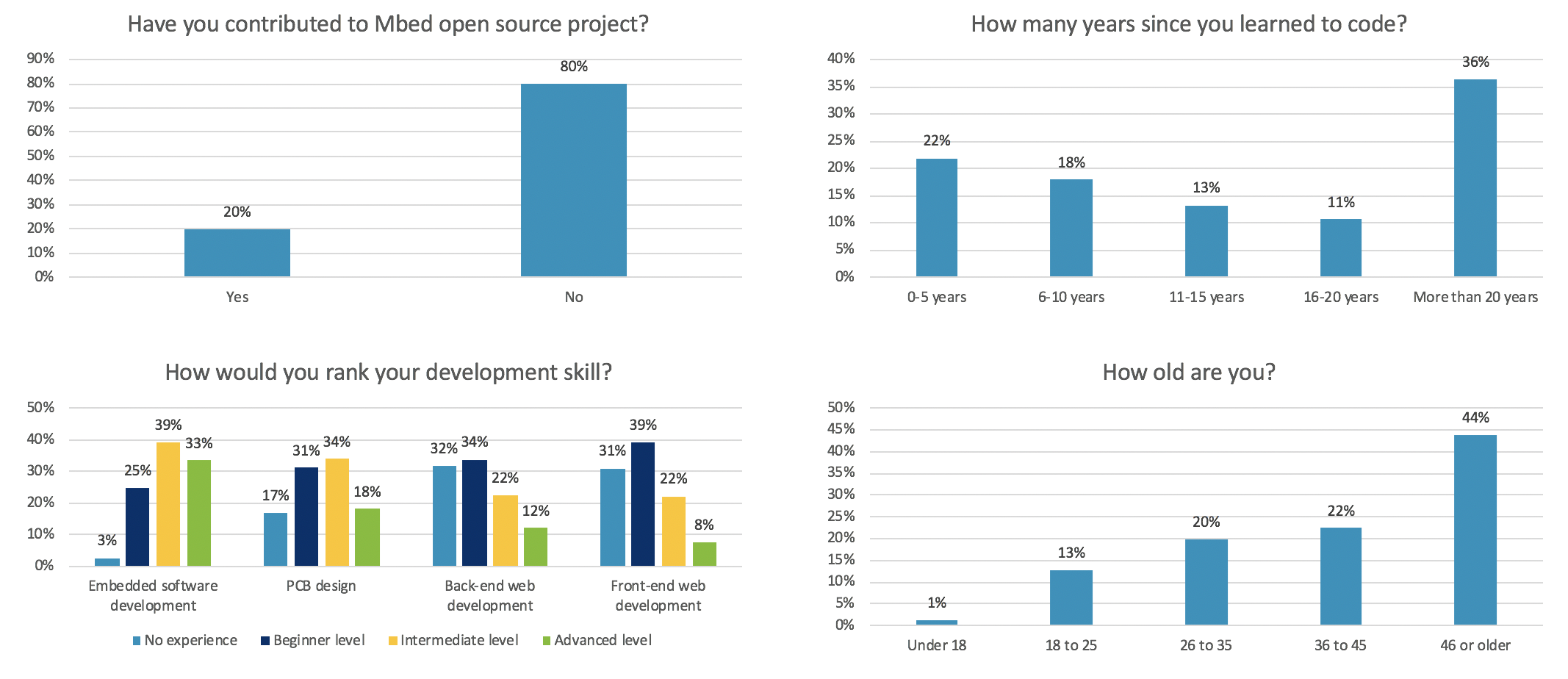
Embedded development is a tough skill to master: from quirky peripherals to manual memory management, trying to squeeze the last bit of performance out of a microcontroller and saving another 20 cents in the bill of materials (BOM) requires experience. 60% of Mbed developers have over 10 years of experience, and almost half the respondents are over 46.
The full-stack embedded developer seems to be upcoming, with 30% of developers indicating that they can do both sides of an IoT product: both embedded and web.
Mbed demographics
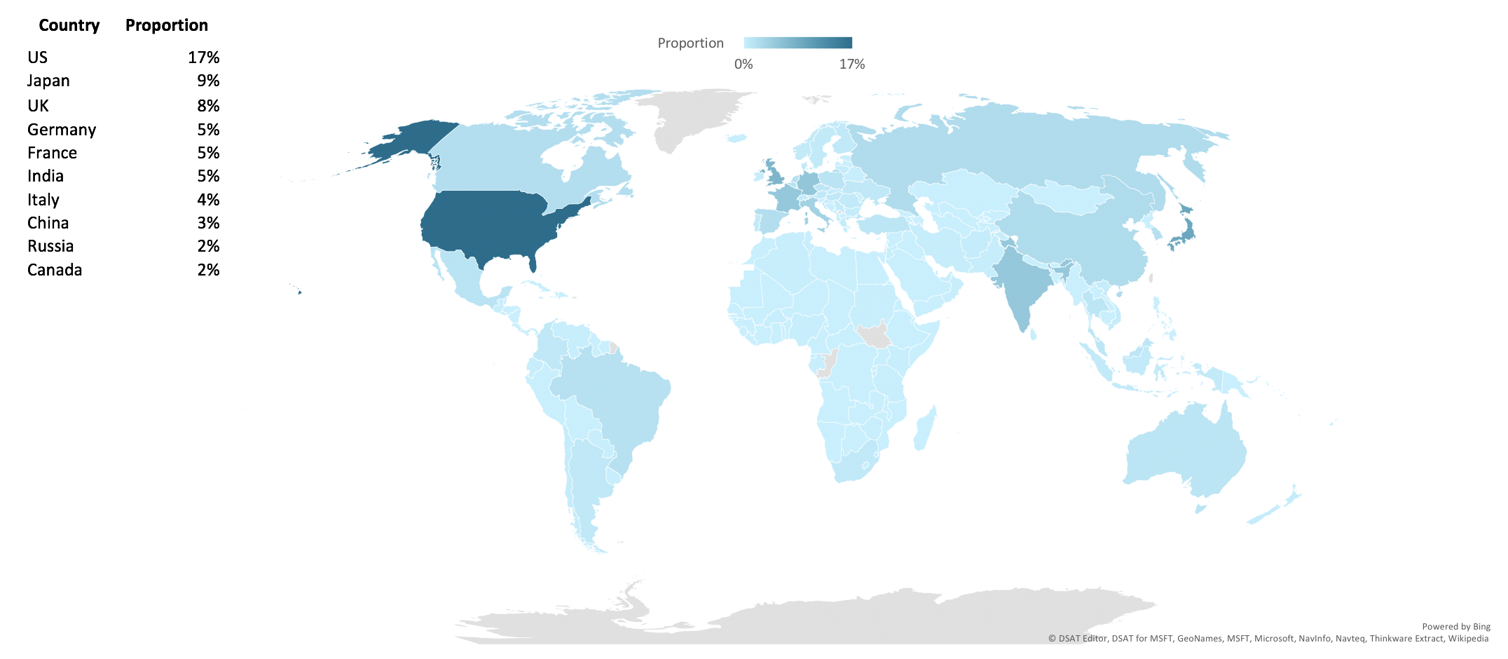
Japan has always been one of the strongest markets for Mbed, but it also sees many developers from the US, UK, Germany, France and India. It's also interesting to see that the results are well balanced between Asia, Europe and North America. However the survey results are skewed toward English speaking countries, probably because the survey was in English.
Mbed developers by country
What are they using?
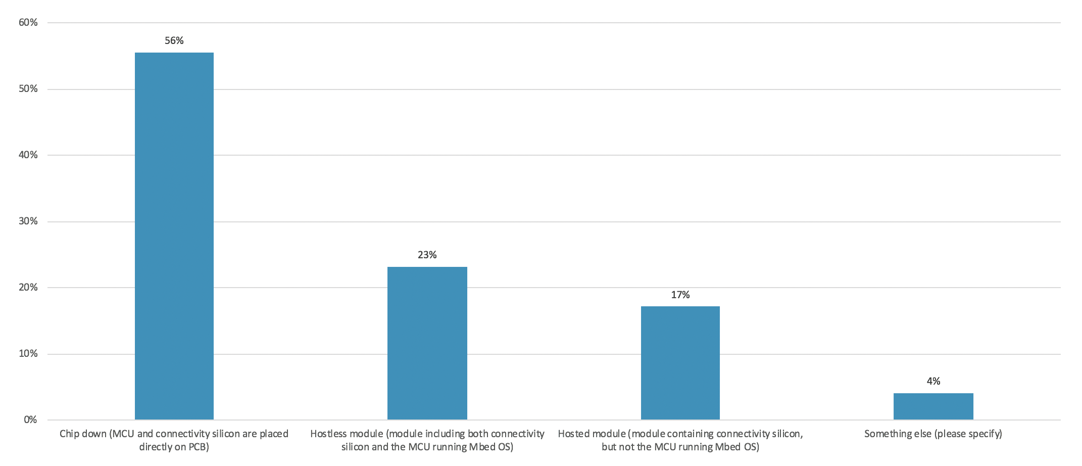
2018 saw a big increase of supported modules in Mbed. Modules drastically shorten the time to market, reduce cost in smaller production runs and can save time by having precertified RF. This trend shows up in survey with 40% of developers incorporating a module in their design.
Hardware architecture
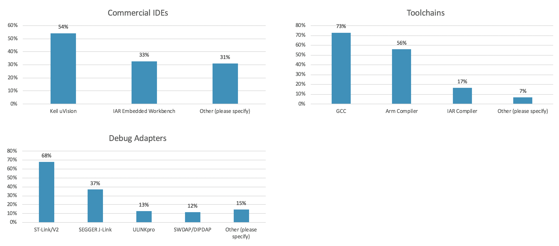
The Arm Mbed Online Compiler is what draws most people into Mbed, but after initial prototyping, most professional developers move their project to their favorite IDE. Keil uVision is the most used IDE among developers, but the high use of GCC over commercial compilers stands out. J-Link is used more than ULINKpro, but Mbed's own open-source SWDAP debugging probe is increasing in popularity.
IDEs and debugging probes used
Connectivity types
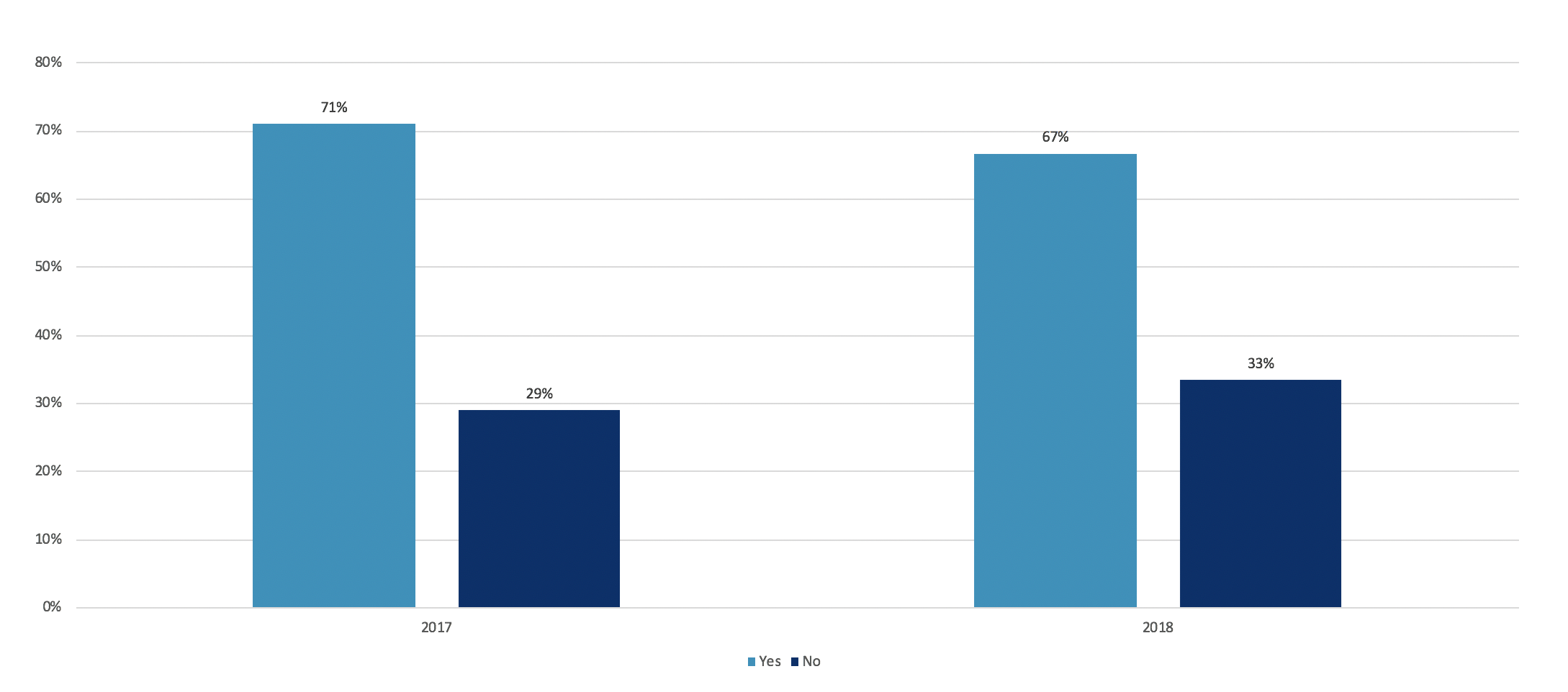
Embedded news is all about IoT, but about 30% of embedded devices still have no connectivity method. That number has increased from 29% to 33%, though it's difficult to draw conclusions. 
Connectivity used in your device?
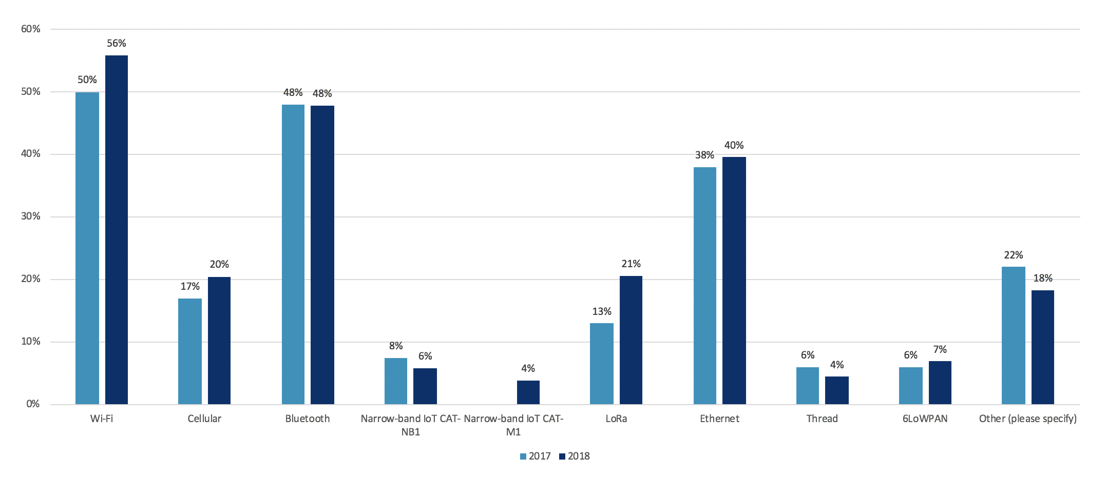
For the devices that use connectivity, mbed sees a very sharp rise of LoRa, now twice as big as the cellular LPWAN methods (Cat-M1 and NB-IoT) combined. Mbed always has had a big foothold in the LoRa community, and it has added a LoRaWAN stack to Mbed OS.
Connectivity by type
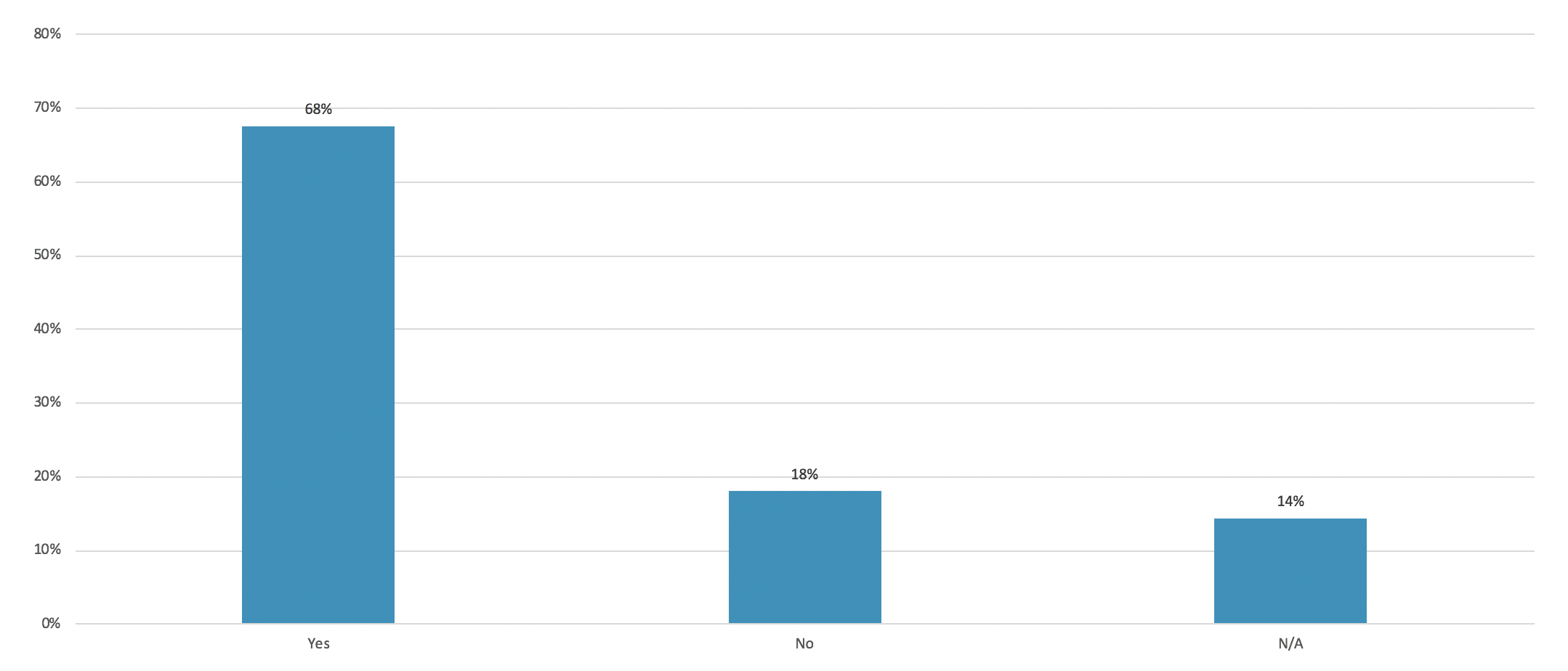
68% of respondents also indicated that security has become more important.
Has security become more important
End markets and going to production
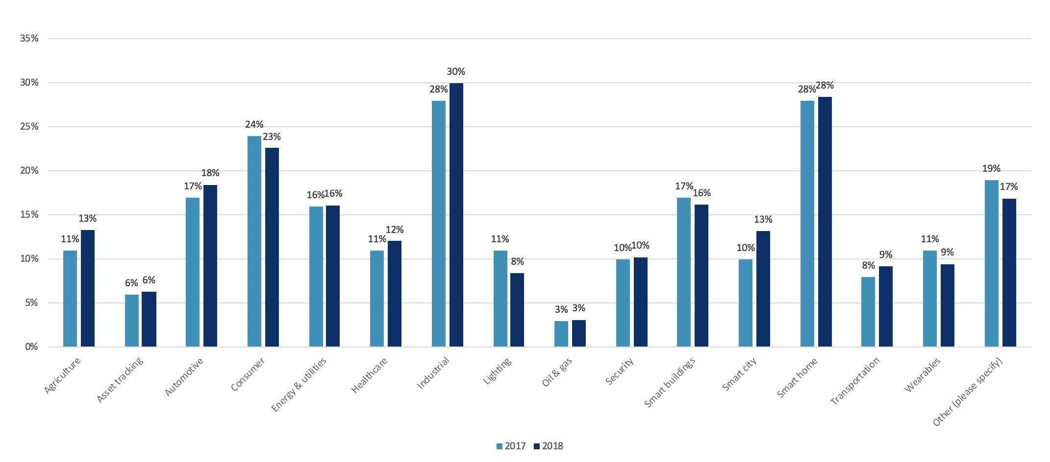
There weren’t a lot of changes in the end markets for which people develop. The industrial and smart home markets remain very strong, the wearables market is slowly dropping and the smart cities market is on the rise. There is a correlation between the growth of LPWANs and smart cities, so if the growth of LoRa, NB-IoT and CAT-M1 continues, it will be interesting to see whether smart cities adoption accelerates, as well.
/media/uploads/janjongboom/survey18-8.png
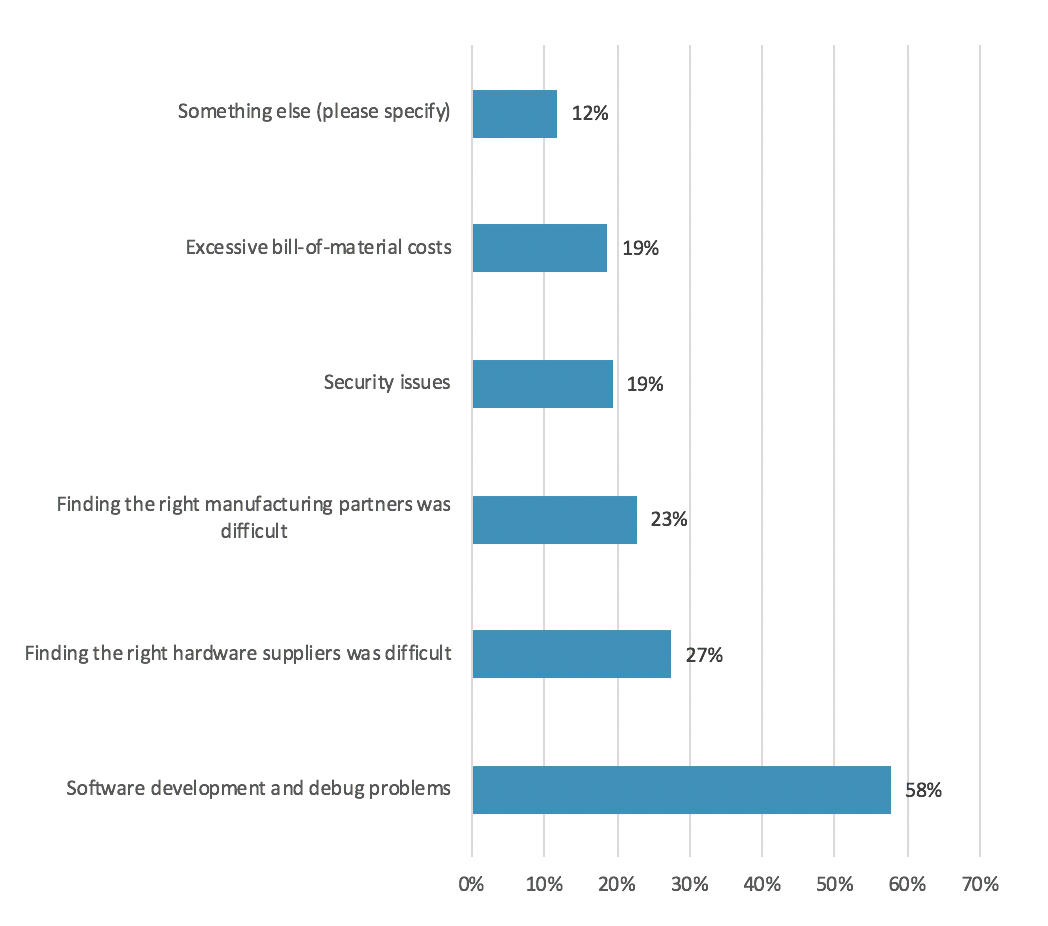
Of course, the only way for IoT devices to affect these end markets is for the device to make it to the market. 16% of users said that they’re currently shipping products, and 24% of respondents expect the product they're working on to go to production. Of the devices in production, respondents identified 'software development and debug problems' as the biggest issue during development. That’s probably not too surprising given that it's mostly developers responding to the survey.
Issues faced when going to production
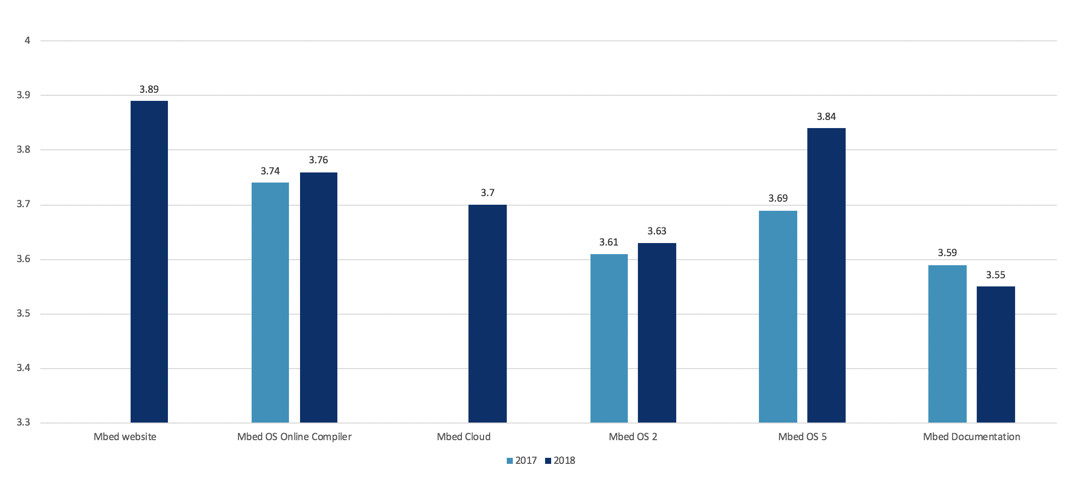
Mbed OS 5 has now been on the market for almost two years, the past year has seen a resilient file system, better networking stacks, bootloader support and new, low power APIs. Satisfaction ratings
One negative point was the low score for documentation, and mbed says it will be working hard to improve the docs with new porting guides and architecture references as well as a general cleanup of old documentation.