All the latest quantum computer articles

See the latest stories on quantum computing from eeNews Europe

Monday, December 31, 2018

128Mbit embedded MRAM for IoT chip designs

By Nick Flaherty www.flaherty.co.uk

A research team at Tohoku University has successfully developed 128Mb-density STT-MRAM (spin-transfer torque magnetoresistive random access memory) with a write speed of 14 ns for use in embedded memory applications, such as cache in IoT and AI. 

This is currently the world's fastest write speed for embedded memory application with a density over 100Mb and will pave the way for the mass-production of large capacity STT-MRAM.

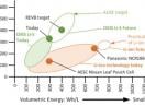
STT-MRAM is capable of high-speed operation and consumes very little power as it retains data even when the power is off. Because of these features, STT-MRAM is gaining traction as the next-generation technology for applications such as embedded memory, main memory and logic. Three large semiconductor fabrication plants have announced that risk mass-production will begin in 2018.

As memory is a vital component of computer systems, handheld devices and storage, its performance and reliability are of great importance for green energy solutions.

The current capacity of STT-MRAM is ranged between 8Mbit to 40Mbit, but to make STT-MRAM more practical, it is necessary to increase the memory density. The team at the Centre for Innovative Integrated Electronic Systems (CIES) has increased the memory density of STT-MRAM by intensively developing STT-MRAMs in which magnetic tunnel junctions (MTJs) are integrated with CMOS. This will significantly reduce the power-consumption of embedded memory such as cache and eFlash memory.

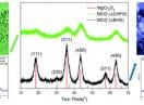
MTJs were miniaturised through a series of process developments. To reduce the memory size needed for higher-density STT-MRAM, the MTJs were formed directly on via holes - small openings that allow a conductive connection between the different layers of a semiconductor device. By using the reduced size memory cell, the research group has designed 128Mb-density STT-MRAM and fabricated a chip.

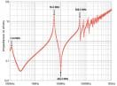
In the fabricated chip, the researchers measured a write speed of subarray. As a result, high-speed operation with 14ns was demonstrated at a low power supply voltage of 1.2 V. To date, this is the fastest write speed operation in an STT-MRAM chip with a density over 100Mb in the world.


Top stories in 2018 on the Embedded blog

By Nick Flaherty www.flaherty.co.uk


Naturally the Internet of Things runs as a theme through the top stories through the year. But we started in January with a standard for high speed SD cards that can be used for embedded storage. And this push into embedded is driving significant growth in microcontrollers - we know this, but its good to have the numbers

New tools for crypto and GUI development were if distinct interest, but we also saw significant interest from some applications, particularly a solar powered autonomous camera and a sprayable antenna that can be easily deployed for wireless IoT nodes.  

AI is also a strong theme, as MIPS and Wave Computing drive chips and Tuya and Microsoft drive services, while Infineon's backing of FreeRTOS will boost the use of the open source real time operating system.

The year finished strongly with the industrial IoT rollout across ports around the world, and we look forward to covering the fantastic technologies that are emerging for the embedded market in 2019. 

  1. JEDEC doubles SD card speeds
  2. MISRA-compliant embedded crypto tools target the IoT
  3. MIPS rides the AI wave
  4. Microsoft pushes harder into IoT
  5. ST buys Draupner Graphics for GUI tech in the HMI of Things
  6. Zephyr adds SiFive for RISC-V support
  7. Researchers incorporate optoelectronics into washable fabrics
  8. Tuya aims to drive AI for the IoT
  9. Embedded drives microcontroller growth
  10. Infineon backs FreeRTOS for IoT
  11. Sprayable, transparent antennas for the IoT
  12. Solar powered autonomous camera
  13. Ports trial IoT tech 


Four team for WiFI sensing in smart homes

By Nick Flaherty www.flaherty.co.uk

Cognitive Systems in Canada has teamed up with Plume and Qualcomm Technologies to work with Stanley Black & Decker on a smart home security system called Omni. 

This would use Cognitive's Aura WiFi Motion technology, Plume’s cognitive software and OpenSync device software stack, and Qualcomm’s Mesh Networking Platform. The result is a self-install security and motion detection system that alerts end users to motion in and around their homes and businesses without the privacy risks, set-up hassles or high costs that come with security cameras and sensors. The collaboration between the four is a key step towards creating a truly cognitive, smart home or business.

“With more than 35 patents granted, we are very well positioned to disrupt the smart home industry by providing motion detection for security applications and elder care, and most notably, the vital context needed to make a truly smart home,” said Taj Manku, Co-Founder and CEO at Cognitive Systems. “Our WiFi Motion software stack allows Stanley Black & Decker’s Omni to provide motion detection coverage across an entire home or business, without cameras, so that users know their locations and loved ones are safe and secure.”

The Aura WiFi Motion technology uses RF sensing technology that can “see” and interpret WiFi signals, coupled with predictive analytics for reliable and accurate detection and localization of motion.

Cognitive’s solution integrates with OpenSync, an open source embedded software that allows partners like Cognitive to launch applications to a ready-made audience across millions of homes. OpenSync intelligently processes data collected by Omni in the Plume Cloud and enables new services to be deployed, managed and supported.

“As the IoT landscape changes with more devices and use-cases, customers are increasingly looking for new service providers to enter the home and bring new solutions over-the-top,” said Tyson Marian, Chief Commercial Officer at Plume. “Omni is a great example of how we enable partners to provide new WiFi applications and monetise their services leveraging our existing service portfolio to deliver performance and insightful data at scale.”

Omni will be available for purchase in the summer of 2019 but will be shown at CES in Las Vegas next week.. “Our goal is to provide our customers with a security product that provides true peace of mind,” said Spencer Maid, Vice President, Breakthrough Innovation at Stanley Black & Decker. “Cognitive Systems’ Aura WiFi Motion technology, combined with Adaptive WiFi delivered through Plume’s cognitive service curation platform, allows true interoperability between IoT devices to ensure motion is monitored and interpreted effectively, enabling customers to not only protect their homes and businesses, but also keep their privacy intact.”


Top stories in December

By Nick Flaherty www.flaherty.co.uk

This month has seen significant interest in the implementation of the Internet of Things for industrial applications (IIoT). The roll out of IoT in several ports around the world is showing the increasing robustness of the technology and driving interest. The use of IP from Ceva for a low power Bluetooth 5 system-on-chip that can use energy harvesting is also helping to boost the delivery of IIoT capability.

The roll out of I3C is also being boosted with a royalty free version of the basic implementation, but still a premium for the rest of the functionality.

Thursday, December 27, 2018

Single chip Bluetooth 5 transceiver for IoT

By Nick Flaherty www.flaherty.co.uk

InPlay Technologies has licensed and deployed CEVA's RivieraWaves Bluetooth Low Energy (BLE) IP in its latest SwiftRadio SoC.

The 55nm single chip is aimed at wearables, healthcare, industrial, VR/AR and the internet of things (IoT) with the mature RW-BLE5 IP from CEVA together with InPlay's ultra-low power RF and its proprietary multi-mode collaborative protocols providing Rx sensitivity of -97.5dBm and sleep current as low as 500nA.

The SoC integrates a high-performance Arm Cortex-M4F microprocessor and subsystem with a floating-point processing unit, 256KB ROM and 64KB SRAM, and peripherals such as I2C, UART, SPI, I2S, PDM, PWM and keyboard controllers. It also has built-in hardware security engines such as AES256, SHA256 and ECC256 and supports authenticated secure boot.

"The SwiftRadio IN6xx enables a paradigm shift in the Bluetooth Low Energy based wireless applications, opening up incredible new opportunities and use cases for this technology," said Jason Wu, CEO of InPlay. "Our extensive mixed signal and RF design expertise along with the low power architecture of CEVA's RW-BLE5 IP and the advanced process technology from UMC has allowed us to deliver a best-in-class product for this burgeoning market."

"UMC has developed a deep portfolio of specialty process technologies engineered to serve the fast-growing market for IoT, AI, Auto & Smartphone products, including sophisticated low power solutions that integrate embedded flash technology," said Steven Liu, vice president of Corporate Marketing division at UMC. "We are pleased to partner with InPlay to enable the innovative features of their SwiftRadio SoC, which utilizes our 55nm ultra Low Power (uLP) embedded flash platform to address uLP market needs of portable products that require extended battery life while maintaining high performance."

"We are delighted to announce InPlay as a licensee for our Bluetooth 5 IP," said Aviv Malinovitch, vice president and general manager of the Connectivity Business Unit at CEVA. "We look forward to seeing the SwiftRadio products in the market, ensuring exceptional performance for power- and price-sensitive wireless IoT devices."

Friday, December 21, 2018

Camera films motion of electrons

By Nick Flaherty www.flaherty.co.uk


A team from the Institute of Experimental and Applied Physics at Kiel University (CAU), under the direction of Professor Michael Bauer and Professor Kai Roßnagel, are investigating the energy exchange of the electrons with their environment in real time, and thereby distinguishing individual phases. 

In their experiment, they irradiated graphite with an intense, 7 femtosecond light pulse and filmed the impact on the behaviour of electrons.  A second, delayed light pulse releases some of these electrons from the solid.  

A comprehensive understanding of the fundamental processes involved could be important in future for applications in ultrafast optoelectronic components. 

The properties of a material depend on the behaviour of its constituent electrons and atoms. A basic model to describe the behaviour of electrons is the concept of the so-called Fermi gas, where the electrons in the material are considered to be a gaseous system. In this way, it is possible to describe their interactions with each other. 

The resolution of 13 femtoseconds makes it one of the fastest electron cameras in the world. "Thanks to the extremely short duration of the light pulses used, we are able to film ultrafast processes live. Our investigations have shown that there is a surprising amount of stuff happening here," said Michael Bauer, professor of ultrafast dynamics at the CAU. He developed the system, together with the working group of Kai Roßnagel, professor of solid state research with synchrotron radiation.

In their current experiment, the research team irradiated a graphite sample with a short, intense light pulse of only seven femtoseconds duration. Graphite is characterised by a simple electronic structure. Thus, fundamental processes can be observed particularly clearly. In the experiment, the impacting light particles - also called photons - disturbed the thermal equilibrium of the electrons. This equilibrium describes a condition in which a precisely-definable temperature prevails amongst the electrons. The Kiel research team then filmed the behaviour of the electrons, until a balance was restored after about 50 femtoseconds.

In doing so, the scientists observed numerous interaction processes of excited electrons with the impacting photons, as well as atoms and other electrons in the material. On the basis of the film footage, they could even distinguish different phases within this ultrashort period: first of all, the irradiated electrons absorbed the light energy of the photons in the graphite, and thereby transformed it into electrical energy. Then the energy was distributed to other electrons, before they passed it on to the surrounding atoms. In this last process, the electrical energy is ultimately permanently converted into heat; the graphite warms up.

The experiments of the Kiel research team also confirm theoretical predictions for the first time. They enable a new perspective on a research topic which has hardly been investigated on this short time scale. "Through our new technical possibilities, these fundamental, complex processes can be observed directly for the first time," said Bauer. This approach could also be applied in the future to investigate and optimise ultrafast motions of light-agitated electrons in materials with promising optical properties.

Production-ready AI chip has embedded MRAM magnetic memory

By Nick Flaherty www.flaherty.co.uk

Gyrfalcon Technology Inc. (GTI) has launched the first production chip for machine learning with embedded MRAM non-volatile magnetic memory.

The 22nm Lightspeeur 2802M is aimed at IoT endpoints, cloud solutions, autonomous vehicles and many other use cases in edge AI. It has 40MB of memory which can support large AI models or multiple AI models. Examples of models that could be supported within the same chip are image classification, voice identification, voice commands, facial recognition, pattern recognition and many others.

“Our proprietary and patented MRAM engine allowed us to bring this first of our company’s many planned MRAM-enabled AI Accelerators to market, to open up new use cases and drive the success of our customers’ product designs,” said Terry Torng, GTI Co-Founder and SVP of Engineering.

The 2802M is the first in a portfolio of MRAM chips in the company’s roadmap using the MPE and APiM technologies. MPE (Matrix Processing Engine) uses CNN with the APiM (AI Processing in Memory), pairing logic with memory like a real human brain. This optimises the speed of processing, achieving high TOPS performance, while also saving tremendous amounts of power by avoiding management of data in discrete memory components.

The MRAM line of chips will use the SDK and the recently announced PLAI Builder from other of the company's AI chips, which simplifies AI Model creation for development teams less familiar with developing solutions using artificial intelligence. AI Models created with Caffe, TensorFlow and other tools can be supported, enabling a wide variety of neural networks, including VGG, MobileNet, ResNet, SDD, ImageNet and others.

“We are pleased to work with an innovative company like Gyrfalcon Technology to create further growth in the AI space,” said Brad Paulsen, Senior Vice President of TSMC North America. “TSMC’s embedded MRAM process enables unique product differentiation in both the Automotive and AIoT markets.”

www.gyrfalcontech.ai.

Tunable origami RF filters block a large range of frequencies

By Nick Flaherty www.flaherty.co.uk

Researchers at the Georgia Institute of Technology have used an origami-based structure to create radio frequency filters that have adjustable dimensions, enabling the devices to change which signals they block throughout a large range of frequencies.

The new approach to creating these tunable filters could have a variety of uses, from antenna systems capable of adapting in real-time to ambient conditions to the next generation of electromagnetic cloaking systems that could be reconfigured on the fly to reflect or absorb different frequencies.

The team focused on one particular pattern of origami, called Miura-Ori, which has the ability to expand and contract like an accordion.

“The Miura-Ori pattern has an infinite number of possible positions along its range of extension from fully compressed to fully expanded,” said Glaucio Paulino, the Raymond Allen Jones Chair of Engineering and a professor in the Georgia Tech School of Civil and Environmental Engineering. “A spatial filter made in this fashion can achieve similar versatility, changing which frequency it blocks as the filter is compressed or expanded.”

The researchers used a special printer that scored paper to allow a sheet to be folded in the origami pattern. An inkjet-type printer was then used to apply lines of silver ink across those perforations, forming the dipole elements that gave the object its radio frequency filtering ability.

“The dipoles were placed along the fold lines so that when the origami was compressed, the dipoles bend and become closer together, which causes their resonant frequency to shift higher along the spectrum,” said Manos Tentzeris, the Ken Byers Professor in Flexible Electronics in the Georgia Tech School of Electrical and Computer Engineering.

To prevent the dipoles from breaking along the fold line, the perforations were suspended at the location of each silver element and then continued on the other side. Additionally, along each of the dipoles, a separate cut was made to form a “bridge” that allowed the silver to bend more gradually. For testing various positions of the filter, the team used 3D-printed frames to hold it in place.

The researchers found that a single-layer Miura-Ori-shaped filter blocked a narrow band of frequencies while multiple layers of the filters stacked could achieve a wider band of blocked frequencies.

Because the Miura-Ori formation is flat when fully extended and quite compact when fully compressed, the structures could be used by antenna systems that need to stay in compact spaces until deployed, such as those used in space applications. Additionally, the single plane along which the objects expand could provide advantages, such as using less energy, over antenna systems that require multiple physical steps to deploy.

“A device based on Miura-Ori could both deploy and be re-tuned to a broad range of frequencies as compared to traditional frequency selective surfaces, which typically use electronic components to adjust the frequency rather than a physical change,” said Abdullah Nauroze, a Georgia Tech graduate student who worked on the project. “Such devices could be good candidates to be used as reflectarrays for the next generation of cubesats or other space communications devices.”

There were also physical advantages to using origami.

“The Miura-Ori pattern exhibits remarkable mechanical properties, despite being assembled from sheets barely thicker than a tenth of a millimeter,” said Larissa Novelino, a Georgia Tech graduate student who worked on the project. “Those properties could make light-weight yet strong structures that could be easily transported.”


Thursday, December 20, 2018

IIC swallows OpenFog to drive fog and edge computing

By Nick Flaherty www.flaherty.co.uk

The Industrial Internet Consortium is to absorb the OpenFog Consortium to boost specifications for Industrial IoT, fog and edge computing. The move will bring OpenFog members into the IIC organisation at a time when their complementary areas of technology are emerging in the mainstream.

The combined memberships will continue to drive the momentum of the Industrial Internet including the development and promotion of industry guidance and best practices for fog and edge computing. The organisations expect the details to be finalised in early 2019.

“This is great news for the industry. Both organisations have been advancing the IIoT, fog and edge computing, and their members represent the best and the brightest in their fields. It makes sense to merge their expertise and work streams to continue providing the IIoT, fog and edge guidance that the industry needs,” said Christian Renaud, Research Vice President, Internet of Things, 451 Research.

“The Industrial Internet Consortium, now incorporating OpenFog, will be the single largest organisation focused on IIoT, AI, fog and edge computing in the world. Between both of our organisations we have a remarkable global presence with members in more than 30 countries,” said IIC President Bill Hoffman. “This agreement will help accelerate the adoption of the IIoT, fog and edge computing.”

The Industrial Internet Consortium is the world’s leading membership program transforming business and society by accelerating the Industrial Internet of Things. The OpenFog Consortium was founded at the end of last year to advance fog computing and address bandwidth, latency and communications challenges associated with IoT, 5G and AI applications.

“We’re excited by the growth and advancement of fog technologies–from a technology, standards and general awareness standpoint—since our launch nearly three years ago,” said Matt Vasey, OpenFog chairman and president, and director, AI and IoT business development, Microsoft. “During that time, it has increasingly become apparent that we share so much synergy with the efforts of the IIC that it just made sense to bring the two consortia together. The resulting combination of memberships, resources and shared knowledge will only further the growth of the technologies, including fog, that will support IIoT ecosystems.”

www.iiconsortium.orgwww.openfogconsortium.org

Related stories:

MIPS goes open source without royalties

By Nick Flaherty www.flaherty.co.uk

In a dramatic step, Wave Computing, the new owner of MIPS, has made the 32bit and 64bit instruction set architecture (ISA) open source without licensing fees or royalties.

This follows the success of the RISC-V open source architecture that is similar. Under the MIPS Open program, participants will have full access to the most recent versions of the 32-bit and 64-bit MIPS ISA free of charge. Participants in the MIPS Open program will also be licensed under MIPS’ hundreds of existing worldwide patents. 

“Having spent years in the open source technology movement, I can attest to the hunger for community-driven solutions,” said Art Swift, president of Wave Computing’s MIPS IP Business. “However, until now, there has been a lack of open source access to true industry-standard, patent-protected and silicon-proven RISC architectures. The overwhelmingly positive response we have received thus far from customers on our MIPS Open initiative is an indication of the dramatic, positive impact we believe the program will have on the industry. We invite the worldwide community to join us in this exciting journey and look forward to seeing the many MIPS-based innovations that result.”

“The MIPS Open initiative is a key part of Wave’s ‘AI for All’ vision,” said Lee Flanagin, Wave’s senior vice president and chief business officer. “The MIPS-based solutions developed under MIPS Open will complement our existing and future MIPS IP cores that Wave will continue to create and license globally as part of our overall portfolio of systems, solutions and IP. This will ensure current and new MIPS customers will have a broad array of solutions from which to choose for their SoC designs, and will also have access to a vibrant MIPS development community and ecosystem.”

The MIPS ISA represents decades of robust innovation with over 8.5 billion MIPS-based chips having shipped in thousands of commercial designs to-date, from the standalone MIPS company through its ownership by Imagination Technologies. Wave has been working on a chip for artificial intelligence (AI) from the edge to the data centre, and Wave CEO Derek Meyer was a key executive at MIPS.

“This is a major milestone not only in the history of our two companies, but also for the AI compute industry,” said Meyer back in June when the company acquired MIPS. “With working DPU commercial silicon and being in the final stages of bringing our first AI systems to market, now is the time for us to expand to the Edge of Cloud. The acquisition of MIPS allows us to combine technologies to create products that will deliver a single ‘Datacentre-to-Edge’ platform ideal for AI and deep learning. We’ve already received very strong and enthusiastic support from leading suppliers and strategic partners, as they affirm the value of data scientists being able to experiment, develop, test and deploy their neural networks on a common platform spanning to the Edge of Cloud.”

The MIPS Open initiative will further fuel the adoption of MIPS by encouraging the global semiconductor community to develop new, MIPS-compatible solutions for a variety of emerging market applications. The MIPS Open initiative will be moderated by Wave Computing and an Advisory Committee that will include industry-leading OEMs, partners, universities and technology luminaries who will help guide community-driven innovations on MIPS. The MIPS Open initiative will also include certified verification partners who will assist in ensuring compatibility of implementations and preventing architectural fragmentation.

The MIPS Open initiative will help greatly expand the existing MIPS ecosystem comprised of thousands of developers and over 100 academic institutions worldwide by offering new opportunities to create innovative solutions from third-party tool vendors, software developers and universities. Through the MIPS Open program, MIPS customers will be assured that development tools, applications, or other value-added features and services provided by the MIPS Open ecosystem will be compatible with new implementations.

A downloadable MIPS architecture, licensing details, support mechanisms, and information on how to participate will be announced in Q1 2019.

Developers, partners and companies seeking additional information on the MIPS Open initiative can visit https://www.wavecomp.ai/mipsopen.