All the latest quantum computer articles

See the latest stories on quantum computing from eeNews Europe
Showing posts with label silicon. Show all posts

Friday, September 09, 2016

Sequans to deliver LTE IoT chip for roll outs

By Nick Flaherty www.flaherty.co.uk

IoT chipmaker Sequans Communications is demonstrating its LTE-M and LTE-NB chips this week ready for roll out of systems later this year.

The Monarch chip is being shown linked to an LTE eNodeB base station emulator, the Amari OTS 100 from Amarisoft. This is an LTE Cat M1/NB1, LTE Release 13 design specifically for narrowband IoT applications, including sensors, wearables, and other low data, low power M2M and IoT devices. Monarch complies with the ultra-low-power and reduced complexity feature requirements of the 3GPP release 13 LTE Advanced Pro standard, defining narrowband, low data rate LTE technology for machine (M2M) communications.


The baseband, RF transceiver, power management, and RAM memory are integrated into a single 6.5 x 8.5 mm package (which is not necessarily a single chip), and also has programmable RF filtering for global band support. Sequans' proprietary dynamic power management technology will give it an operating life of over 10 years, says the company, overcoming one of the main objections in using LTE for IoT (the other being the operator costs)

Category M1, also known as LTE-M and Cat M, delivers about 1 Mbps maximum in a 1.4 MHz channel, and Category NB1, also known as narrowband IoT, or NB-IoT, delivers about 40 kbps in a 200 kHz channel.

“We are very proud to highlight the key capabilities of Monarch in this first-in-the-industry live demo of a Cat M1/NB1 chip,” said Georges Karam, CEO of Sequans. "In designing Monarch, we worked from day one to make sure it would be fully optimized in both cost and power consumption to fully unleash the LTE for IoT market potential. I am very excited to say that Monarch is operating as designed and we expect to have it ready for network deployments in Q4. Monarch is an entirely new, fully-optimized silicon design, and not an earlier generation chip modified with software to simulate Cat M1 and NB1 capabilities, as others appear to be doing.

He says the company is closely engaged with major operators, major eNodeB vendors, and key technology partners to fully address deployment plans for Cat M1 and NB1 networks, beginning first in the US (it has a deal with Verizon). Several OEMs and ODMs are developing modules and devices, with applications including health and fitness wearables, smart energy meters and asset trackers, industrial monitors and sensors, and Sequans has teamed up with Gemalto for the security and authentication element.

According to ABI Research, a leader in technology market intelligence, cumulative cellular M2M module shipments from 2016 through 2021 will reach 1.1 billion units; LTE modules will experience the highest growth, exceeding 50 percent of all cellular M2M shipments in 2021.

“With the recent ratification of the Cat M1 and Cat NB1 standards, it is pretty clear that LTE will rapidly replace 2G and 3G connections in the major M2M markets,” said Dan Shey, Managing Director and Vice President at ABI Research. “Sequans’ introduction of its Cat M1/NB1 chip, already working and being developed rapidly by Sequans in close collaboration with leading operators and OEMs, shows the strong momentum developing behind LTE Cat M1 and Cat NB1.”

“Narrowband LTE technology is of crucial importance to the M2M and IoT markets as many use cases will require nation-wide and carrier-grade connectivity. Our Monarch chip is an ideal solution to address this demand,” said Karam.

Tuesday, August 09, 2011

TI introduces industry’s lowest power NFC transceiver

The TRF7970A evaluation module 
By Nick Flaherty www.flaherty.co.uk

TRF7970A NFC platform speeds designs with easy-to-configure software

Texas Instruments has launched what it claims is industry’s lowest-power contactless short-range communication transceiver. Aimed at infrastructure devices, the TRF7970A extends battery life through eight selectable power modes ranging from under 1µA in power-down mode to 120mA in full-power mode. This gives it twice the battery life of competing products, says TI.
The transceiver comes with easy-to-configure software to help developers get started quickly. Royalty-free stacks are compatible across a broad range of ultra-low-power MSP microcontrollers. Additionally, developers are able to directly access all control registers, allowing for easy fine-tuning of various parameters for the highest performance in every application.
The new transceiver builds on TI’s platform of RFID products by supporting peer-to-peer communication and card emulation in addition to reader/writer capability while maintaining pin-for-pin compatibility with the previous TRF7960. Peer-to-peer communication continues to increase in popularity in applications including medical equipment, secure pairing and payments. This allows users to more easily take advantage of continuously evolving features and apps. For example, NFC devices can configure Wi-Fi and Bluetooth technology sessions between devices without consumer interaction, share and interact with feature- and content- rich data such as coupons at point of sale, and allow consumer devices to easily exchange files and contacts.

Features and benefits:
  • Eight selectable power modes (Power modes range from <1 µA to 120 mA)
  • Supports peer-to-peer communication, reader/writer capability and card emulation
  • Supports two crystal oscillator frequencies: 13.56MHz or 27.12MHz frequencies give engineers more flexibility in speed and cost options for their designs
  • Large 128 byte FIFO buffer for NFC communications allows developers using microcontrollers with low MHz to create products capable of handling large data transfers
  • Compliance with ISO/IEC 18092 and ISO/IEC 21481 standards gives developers the ability to create globally interoperable products
  • NFC software stack libraries and an innovative RF field detector allow for easy development efforts and robust, cost effective designs
  • NFC Peer-to-Peer Initiator as well as Active and Passive Target Operation are available for MSP430™ microcontrollers
  • Supports multiple reader/writer protocols and includes demo software stacks for reader/writer mode ISO/IEC 15693, ISO/IEC 18000-3, ISO/IEC 14443A/B and FeliCa
With more than 1 billion RFID tags and more than 100 million RFID reader devices manufactured, TI’s RFID technology is used in a broad range of applications worldwide. Designers can accelerate time to market by tapping into TI's complete software and hardware tools, extensive third-party offerings and technical support.
The TRF7970A NFC development kit is immediately available for order at www.ti.com/nfc-pr-es and priced at USD $99.
Related articles
Enhanced by Zemanta

Wednesday, March 16, 2011

Chipworks reverse engineers the Apple A5 processor

By Nick Flaherty www.flaherty.co.uk

Chipworks has reversed engineered the Apple A5 processor used in the iPad2. 
They decapsulated the A5 a couple of days ago, but as you could see in those early pictures, you can’t tell much of a chip’s layout from the top metal – it’s all power and ground buses.  So they had to de-layer the chip down to a level to see the block layout of the chip; not an easy thing when there’s nine layers of metal!  In fact, these days it’s easier to go in from the back and remove the substrate silicon, and look at the gate level from below.  Then they identify the circuit blocks that make up the full device.
For the A5, a dual ARM core processor:
Apple A5 Polysilicon Die Photo with Annotations
The ARM cores are in the right half of the die, with ~4.5 Mb of cache memory each.  You can also see the USB interface at the top, and the DDR SDRAM interfaces at the bottom right, for the memory in the top part of the package-on-package.  Other I/O blocks are strewn around the edge of the die.
It seems likely that Apple will actually be shipping TSMC-made parts later this year, since Samsung is a competitor with its Galaxy tablet series, but the current devices are made by Samsung, as shown by a cross section of the chip:

Enhanced by Zemanta

Friday, March 04, 2011

Freescale Power Architecture microcontrollers for industrial market mark the end of ColdFire

By Nick Flaherty www.flaherty.co.uk

Freescale Semiconductor is moving its Power Architecture into microcontrollers that effectively marks the end of the ColdFire range for new designs.
The PX series of MCUs is based on Freescale’s e200 Power Architecture cores and is designed to meet the needs of the most complex industrial control applications, including motion control, power generation, clinical medical, aerospace and defence, motor drives, renewable energy, robotics and more.
“This addition to our industrial MCU portfolio is significant because the industrial electronics market can truly benefit from the capabilities of Power Architecture technology,” said Reza Kazerounian, senior vice president and general manager of Freescale’s Microcontroller Solutions Group. “The PX series of Power Architecture MCUs brings unparalleled performance to a broad range of industrial applications and provides the advanced technology and enablement our customers need for their industrial designs.”
The embedded safety architecture in the PX series of Power Architecture MCUs helps developers meet the safety, reliability and environmental requirements of industrial control applications. Integrated features simplify safety approvals for IEC61511 and IEC 61508 (SIL3), FAA DO-178B Level A and FDA Class II to III.
The single-core performance is up to 600 DMIPS, with multicore options and up to 4 MB of embedded flash memory make the PX series ideal for motion control and other complex, real-time control applications. A single chip can control up to six motors, process complex math algorithms and manage more than the typical three communications connections.
Freescale is also providing run-time software, reference designs and tools for rapid prototyping, advanced debug and system modelling. Customers can lower start-up costs by using Freescale run-time software, such as the free MQX RTOS, DSP and motor control libraries and Swell PEG (portable embedded GUI) development suite. Additionally, Freescale Power Architecture MCUs are supported by tools and the safety-certified INTEGRITY RTOS from Green Hills.
Freescale also offers tools for rapid prototyping with the PX series, including:
  • Modular Tower System hardware development platform with QuickStart code initialisation 
  • RAppID Toolbox with links to the MathWorks Simulink environment 
  • FreeMASTER debug GUI 
All families in the PX series are included in the Freescale product longevity program which ensures a minimum of 10 years of device availability (15 years for medical and automotive devices), providing peace of mind for the embedded designer. For more information, go to www.freescale.com/PXseries.


Related articles
Freescale Files for $1.15 Billion IPO (voices.allthingsd.com)
Freescale introduces intelligent sensor for car battery monitoring (physorg.com)
Freescale Boosts Share Of Tablet Processor Market (informationweek.com)


Friday, December 17, 2010

Moving multicore to embedded is key to US competitiveness

By Nick Flaherty www.flaherty.co.uk

The rapid advances in information technology that drive many sectors of the US economy could stall unless there is significant fundamental research and development of parallel computing, says a new report by the National Research Council -- which will drive the move to embedded multicore systems.
Better options for managing power consumption in computers will also be essential for continued improvements in IT performance.
Advances in single-processor, sequential computer microprocessors have enabled computing performance to increase dramatically -- on the order of 10,000 times in the last 20 years but power management and other technological limitations have made it impractical to continue improving computer performance in this way much longer. Parallel computing, therefore, is the only known alternative for improving computer performance without significantly increasing costs and energy usage, the report says.
"The societal and economic impact of computer technology is undeniable, increasing productivity and efficiency and fostering innovation in medicine, defense, entertainment, and communications," said Samuel Fuller, chief technology officer and vice president of research and development for Analog Devices and chair of the committee that wrote the report. "To ensure that computing systems continue to double in performance every few years, we need to make significant changes in computer software and hardware. Investing in research and development of parallel computing offers a clear path forward."
Despite some mainstream successes in parallel computing -- such as the MapReduce programming framework used by Google to process large data sets using thousands of computers -- most parallel computing in use now is limited to comparatively narrow scientific and engineering applications. To enable parallel computing for broader use, new algorithms, programming models, operating systems, and computer architectures will be required, the report says, and research and development in these areas should be pursued.
In particular, advances are necessary to develop new parallel programming methods and supporting computing systems. Although computing hardware such as semiconductor chips that contain eight or more microprocessors have already been developed, software that can keep that many or more processors busy in parallel is not available for most computing applications.
Research and development should also focus on making computer systems more energy efficient, the report says. Power constraints now affect systems ranging from handheld devices to the largest computing data centres. Most computer chips are designed with silicon-based complementary metal oxide semiconductor (CMOS) technology. While the number of devices per CMOS chip continues to double every few years, the technology has essentially reached its limits with regard to power efficiency. Even as new parallel computing models and solutions are found, most future performance will ultimately be limited by energy constraints, the report notes.
It cautions that while parallel computing is the best alternative for improving future performance, there is no guarantee that it will bring rapid advances like those experienced in recent decades, and a number of uncertainties still need to be addressed. Therefore, research and development should also explore fundamentally different alternatives to today's CMOS technology.
The report also recommends developing open interface standards for parallel programming to promote cooperation and innovation in the industry, designing tools and methods for transferring today's sequential computing to parallel applications, and emphasizing parallel computing as part of computer science education.
Enhanced by Zemanta

Wednesday, December 08, 2010

Renesas and green Hills team up for virtualisation for real time control

By Nick Flaherty www.flaherty.co.uk

Renesas Electronics and Green Hills Software are to jointly develop basic software supporting CPU virtualisation technology for real-time control applications as well as a software development environment.
Through the collaboration, Renesas Electronics will develop added functions necessary for the efficient operation of virtualization software enabling high-speed real-time control and improving the usability of the software development environment, incorporating these functions into microcontrollers (MCUs) with V850 CPU core.
Green Hills Software will port the MULTI Integrated Development Environment (IDE), which includes components such as a compiler and a debugger that already support Renesas Electronics’ V850 core. The new CPU virtualisation technology will provide support for software that enables multiple applications to run independently and simultaneously on a single CPU, such as the INTEGRITY real time operating system (RTOS).
The Green Hills IDE will generate compact and high-speed instruction code optimized for the CPU virtualization technology provided by Renesas Electronics’ V850 core. When combined with virtualization software such as INTEGRITY Secure Virtualization, which support safety standards such as IEC 61508, the software development environment will deliver the means to develop and implement with high efficiency applications with excellent functional safety. There are also plans to include support for the emerging ISO 26262 functional safety standard.
Renesas Electronics has been developing CPU virtualisation technology for the V850 architecture to enable control of multiple systems with a single CPU core without mutual interference, allowing high-speed and composite control in fields such as industrial machinery and automotive systems, where real-time control is essential.
Green Hills Software has made a contribution to facilitating design procedures in virtualised environments through its virtualization software and the software development environment.
Renesas Electronics considers a full-fledged software development environment incorporating basic software that allows efficient use of virtualization technology to be essential.
The software development environment will be available through Green Hills Software as part of the MULTI product family.
Enhanced by Zemanta

Wednesday, September 29, 2010

Shipments of Silicon to Jump 23.6 Percent in 2010

By Nick Flaherty www.flaherty.co.uk
Global silicon shipments in terms of square inches will rise to record levels in 2010, according to semiconductor manufacturing market research firm iSuppli.
 
Shipments of silicon for semiconductor manufacturing in 2010 will grow by 23.6 percent year-over-year, reaching 8.9 billion total square inches, up from 7.2 billion square inches in 2009, iSuppli forecasts. By 2014, 12.4 billion total square inches of silicon will be shipped.
However, while this is good news for filling fabs, it doesn't necessarily follow through to the average selling price (ASP) and the health of the industry. There is a fine balance between demand for silicon and production - too much silicon, low prices; too much demand and not enough siliocn - high prices. 
“Following the recession of late 2008 and 2009, chip manufacturers spent the first half of 2010 striving to reverse the damage they had suffered,” said Len Jelinek, director and chief analyst for semiconductor manufacturing and supply at iSuppli. “Visibility in the second half of 2010 remains limited even as the all-important holiday season inches closer. The good news is that barring any new collapse, silicon suppliers will have sufficient orders on the books to carry them through the third and fourth quarters. And while growth in 2011 won’t match the high expansion rate seen in 2010, iSuppli anticipates that the semiconductor industry will require additional increases in silicon shipments of about 13 percent compared to 2010 shipment rates to meet the projected development.”
Outperforming the industry
The demand for silicon in 12-inch wafers continues to rise at a rate that will outperform the industry average for silicon through 2014. In order to maintain growth, however, silicon suppliers must continue to expand 12-inch wafer manufacturing.
Beyond 2010, iSuppli expects to see a greater emphasis on shifting to even more 12-inch wafer manufacturing. Specifically, mixed signal and other technologies will be moving to 12-inch wafers as a result of older 12-inch tools no longer being cost effective for the manufacturing of leading-edge technology products.
Over the next five years, the availability of additional mature manufacturing capacity and tools will accelerate the conversion to 12-inch wafer manufacturing for products such as analog and mixed signal devices.
Enhanced by Zemanta

Thursday, June 03, 2010

Power management chip shortage looms

Remarkable growth over Christmas drives up prices
By Nick Flaherty www.flaherty.co.uk

Strong demand for power management semiconductors in the first half of 2010 has caught suppliers off-guard, spurring shortages and causing prices to rise in the near term, says market researcher iSuppli. This will impact on the design and supply and cost of portable euipment in particular this year.
Revenue for power management semiconductors reached $6.9 billion in the first quarter of 2010, up 2.9 percent from $6.7 billion in the fourth quarter of 2009. Sequential growth in the first quarter is remarkable given that it is weakest period of the year for sales of semiconductors. The growth of the first quarter reflects a continuation of the expansion that started during the last three months of 2009, after the market stalled briefly in the third quarter of last year.

Growth is expected to continue in the second quarter this year, when revenue is set to rise another 7.2 percent to hit $7.4 billion. And although a bigger upward movement occurred during the same time last year—when power management ascended 18.2 percent from $4.4 billion to $5.2 billion—the second quarter in 2010 will deliver the most robust growth for the industry this year.
“The expansion in the first quarter of 2010 took place because of the industry’s move to fulfill order backlogs and to satisfy limited demand, both of which shrank in the wake of the economic slowdown last year,” said Marijana Vukicevic, principal analyst for power management at iSuppli. “In contrast, growth in the second quarter will be fueled by increased activity in a number of areas utilizing power management semiconductors, including consumer electronics, wireless communications and data processing.”


Suppliers beset with shortages; prices to rise

Suppliers now are suffering from a shortage of power semiconductors, mainly because a recovery in demand—which started in the fourth of quarter of last year—has proven to be of a greater magnitude than current operational capacity can handle. Even with the rehiring of workers and the reopening of fab lines, suppliers have been caught off-guard by the resurgent demand and are unable to keep up, iSuppli’s findings show.
Furthermore, inventory levels at distributors decreased by 1.5 days in the fourth quarter of 2009 amid strong sales—a development that induced even more demand, especially for the analogue and discrete components of the market that already were in a state of shortage. The decline in inventory not only will contribute to big delays at the back end, particularly for analog suppliers, but also will serve to increase pricing, iSuppli believes.
And while prices are expected to stabilize in the second half of 2010, the shortage of commodity devices is likely to drive up Average Selling Prices (ASPs) in the first half, affecting buyers in the short term. Essentially, the price increases will persist until supply catches up with demand, iSuppli projections indicate.


Reblog this post [with Zemanta]

Tuesday, May 25, 2010

ST moves to 32nm for networking chips

By Nick Flaherty www.flaherty.co.uk


Industry’s first Serializer-Deserializer (SerDes) IP in 32nm demon to customers 

STMicroelectronics has launched a 32nm technology platform for the design and development of leading-edge application-specific integrated circuits (ASICs) for networking applications. Central to the new 32nm SoC design platform, which implements ST’s 32LPH (Low-Power High-performance) process technology, is the industry’s first Serializer-Deserializer (SerDes) IP available in 32nm ‘bulk’ silicon.
Enabling very large ASIC designs, greater than 200mm2, ST’s new 32nm 32LPH ASIC design platform enables an unprecedented mix of high performance, high complexity, low power consumption and reduced silicon real estate per functional block. The platform is designed to accelerate the development of next-generation networking ASICs used in high-performance applications such as enterprise switches, routers and servers as well as optical cross-connect and wireless infrastructure applications.
“With the introduction of the 32LPH platform, ST is enabling the next generation of equipment for communication infrastructure applications, which requires highly integrated ASICs that can satisfy the increasing demand in performance, while also meeting extremely challenging power consumption and silicon integration goals,” said Riccardo Ferrari, Group Vice President and General Manager of ST’s Networking and Storage Division. “We are extremely encouraged by the strong interest that customers are demonstrating for this platform, which has already gained key design wins.”

ST’s SerDes IP, called S12, is a key piece of intellectual property that has already been successfully demonstrated in labs at selected key customers. The S12 IP is vital for the development of ASICs for networking applications and enables chip-to-chip, chip-to-module and backplane communications in networking equipment designs.
“ST is the first silicon supplier to bring a full design platform in a 32nm bulk-silicon process technology to the communication infrastructure market, including a next-generation predictive ASIC top-down design methodology, together with a full set of proven IP, such as a SerDes and embedded DRAM, successfully developed over many years by ST in previous technology nodes,” said Philippe Magarshack, Technology R&D Group Vice-President, Central CAD & Design Solutions GM, STMicroelectronics. “ST’s Technology R&D center in Crolles, France, has been instrumental in accelerating the completion of the 32LPH platform where low-power technology meets the high-performance requirements of networking applications, while still enjoying all the cost benefits of high-volume manufacturing. In addition, we have partnered with selected EDA vendors to offer networking customers the benefits of a predictable ASIC turnaround time, including fast virtual physical prototyping, and 32nm-class timing, signal and power integrity sign-off.”
The first ASIC prototypes implemented in ST’s 32LPH process technology are expected early in 2011 with production ramp-up in the second half of 2011.
Further Technical Information
ST’s 32LPH (Low-Power High-performance) design platform for networking applications supports up to 10 metallization layers to increase routing efficiency. The platform is based on the 32nm High-K Metal Gate process developed within the framework of the ISDA alliance, but also incorporates specific IP and devices from ST, such as embedded DRAM with 10-Mbit per square millimeter density and Ternary Content Address Memory (TCAM).
A SerDes (Serializer-Deserializer) is normally integrated multiple times (often up to 200) in a single ASIC chip. It enables serial communication between:

  • ICs, or ASICs, on the same electronic printed-circuit board (Chip-to-Chip);
  • ASICs and the Optical Module, which links to remote equipment (Chip-To-Module);
  • ASICs and Physical Interface Module (Chip-To-Module); or
  • ASICs and the system backplane - the backplane is the internal physical rack inside equipment in which all the system cards are mounted.

ST’s S12 IP macro, which is based on ST’s proven SerDes architecture, can be scaled up to eight 12.5-Gbit/s transmit/receive (Tx/Rx) channels per macro. The S12 has been designed with an optimal footprint for flip-chip BGA packages, and will soon be followed by ST’s S14 IP, which can reach up to 14-Gbit/s transmission speed.

Reblog this post [with Zemanta]

Wednesday, May 12, 2010

DNA as the future of silicon chips?

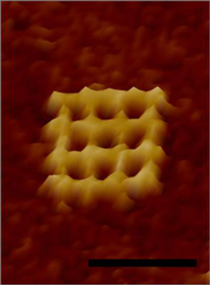
In a single day, a solitary graduate student at a lab bench can produce more simple logic circuits than the world's entire output of silicon chips in a month. So says a Duke University engineer, who believes that the next generation of these logic circuits at the heart of computers will be produced inexpensively in almost limitless quantities in a story at Nanowerk.
In his latest set of experiments, Chris Dwyer, assistant professor of electrical and computer engineering at Duke's Pratt School of Engineering, demonstrated that by simply mixing customized snippets of DNA and other molecules, he could create literally billions of identical, tiny, waffle-looking structures (left). Dwyer has shown that these nanostructures will efficiently self-assemble, and when different light-sensitive molecules are added to the mixture, the waffles exhibit unique and "programmable" properties that can be readily tapped. Using light to excite these molecules, known as chromophores, he can create simple logic gates, or switches. 

More on the story here
Reblog this post [with Zemanta]

Friday, April 30, 2010

NetLogic Microsystems and TSMC Collaborate on 28nm Process Technology

Includes analogue capability for high speed interfaces 
Network processor developer NetLogic Microsystems  is working with leading foundry TSMC to extend their existing collaboration to include TSMC’s NEXSYS 28HP (28nm high performance) semiconductor process node. This will be used for NetLogic’s next-generation knowledge-based processors, multi-core processors and 10/40/100Gigabit PHY.
As an early development partner, NetLogic is using TSMC’s 28nm node to raise networking infrastructure performance and significantly differentiating its product line from the competition.In June 2009 Netlogic bought RMI (Raza Microsystems) to add a range of high performance multicore network processors to its range. 
NetLogic has launched advanced product development for multiple industry-leading product lines on the TSMC 28nm node. The 28HP process offers significant speed, and power efficiency advantages over previous process nodes. In addition, NetLogic Microsystems is developing a suite of custom high-performance circuits optimized around TSMC’s 28nm node, including high-speed serial interface technology, analogue and clocking circuitry, core processing elements and other standard cells, as well as refining the design and tape-out flow for this advanced node.
“By being a consistent early adopter across four generations of process technology, NetLogic Microsystems has consistently provided very high performance and low power products for mission-critical network infrastructure systems,” said Rick Cassidy, president of TSMC North America. “We welcome the extension of our close relationship to include NetLogic Microsystems’ role as an 28nm early technology adopter.”
“We are proud to have been one of the early partners for TSMC in 80nm, 55nm, 40nm and now 28nm for our best-in-class knowledge-based processors, multi-core processors and 10/40/100 Gigabit PHY product families,” said Ron Jankov, president and CEO at NetLogic Microsystems. “By combining the superior design and architecture of our products with TSMC’s proven leadership and track record in advanced manufacturing technologies, we are able to deliver highly innovative products with unprecedented performance, scalability and energy efficiency to our customers.”
NetLogic Microsystems offers high-performance multi-core, multi-threaded processors, knowledge-based processors, content processors, and high-speed 10/40/100 Gigabit Ethernet PHY solutions. These market-leading products are designed into high-performance systems such as switches, routers, wireless base stations, security appliances, networked storage appliances and service gateways to significantly enhance the performance and functionality of next-generation 3G/4G mobile wireless infrastructure, data center, enterprise, metro Ethernet, edge and core infrastructure networks.
Reblog this post [with Zemanta]

Tuesday, April 27, 2010

Dust Networks launches ARM Cortex-M3 system chip for 802.15.4

World's lowest power RF so far

Dust Networks is an intersting company as a leading supplier of wireless sensor networks (WSN). It is using the low power ARM Cortex-M3 processor for a new family of system-on-chips (SoCs) that include an on-chip power amplifier (PA) that will be the basis for a variety of upcoming standards-based WSN products, including IEC 62591 (WirelessHART), 6LOWPAN (IP), and Zigbee PRO products. This is key for the development of the SmartGrid.
The SoCs will feature:
  • A 32-bit ARM Cortex-M3 processor and rich interfaces enable a powerful computing platform while conserving power.
  • The world's lowest power IEEE 802.15.4 radio: a new benchmark is set, with a mere 3 mA transmit at 0 dBm and 3 mA receive current, delivering 5-10 times the battery life of competing technologies, and further expanding the applicability of energy harvesting power sources.
  • Extended range capabilities, with up to 8 dBm output power on-chip PA and an optional external power amplifier.
  • The industry's first IEEE 802.15.4E-ready product, incorporating the emerging standard for time synchronization and channel hopping, while providing legacy support for 802.15.4-2006.

"Our new SoCs are geared to deliver the highest performance while running at a fraction of the power of competing silicon," said Dr. Kris Pister, Chief Technologist at Dust Networks. "In selecting the ARM Cortex-M3 processor for our SoC, we did not have to trade-off performance for power. Dust Networks new IEEE 802.15.4 SoCs will require less than one-tenth of the energy per operation of comparable SoCs."

The level of systems integration in the SoCs is very high, including on-chip power amplifier, DC-to-DC converter, 10 bit ADC and a built in temperature sensor. With configurations up to 512kB of flash and 72kB of RAM, these SoCs will have both the highest computational horsepower of any 802.15.4 chip on the market, and the lowest power consumption. In doze mode, with full processor state and RAM retention, current consumption is under 1uA.

"Low power radios such as IEEE 802.15.4 and wireless mesh networking, epitomized by Dust Networks' TSMP protocol and its "Smart Dust" roots, have transformed the industrial wireless sensor network landscape", said Mareca Hatler, ON World research director. "With the introduction of ultra low power versions of SmartMesh IP (6LoWPAN) systems and ZigBee products, Dust Networks will expand the growing number of 'Smart World' applications that span Smart Buildings, Cities, Government and Homes."

Reblog this post [with Zemanta]

Thursday, December 10, 2009

SDR comes to radio and TV


Microtune has developed a chip architecture that brings Software Defined Radio (SDR) to car radios.
The MT3511 RF MicroDigitizer provides a flexible RF front end for many different standards and is coupled with a digital signal processor for a low cost implemention in a car radio.
For automotive manufacturers, software defined radio (SDR) represents a revolutionary approach to in-vehicle car entertainment, connectivity and multimedia. It enables them to flexibly deliver the most popular consumer features ­AM/FM, digital radio, CD audio, MP3 playback, navigation, as well as connectivity for iPod®, SD card, USB and Bluetooth by using common hardware that is configurable, scalable and upgradable via software. SDR solutions dramatically change ‘infotainment’ business, design and manufacturing models. This technology offers car makers a global radio platform, increased design flexibility, substantial cost-efficiencies and a future-proof migration path to new standards and enhanced features.
The MT3511 is a key front-end component in the SDR architecture. It combines the functions of a state-of-the-art RF tuner and an advanced analogue-to-digital converter in a single miniature chip­it receives and tunes a broadcast signal from a car antenna, and then converts the signal from analog to digital format for processing in software by a DSP or multimedia processor. It also supports world-standard AM/FM, HD Radio technology, digital radio mondiale (DRM), and weather band, and a DAB version with support for the higher frequency L band is being considered.
The advantage is that it replaces multiple hardware-specific components in today’s radio subsystem with a generic hardware platform that reduces design complexity, time-to-market, time-to-qualification and costs.
“For decades, leading automotive manufacturers and Tier-1 suppliers have used Microtune radio and TV tuners to migrate compelling consumer-class entertainment to the car,” said James Fontaine, President and CEO of Microtune. “We are now introducing a single-chip RF-to-digital converter that will help drive software defined radio throughout the auto industry as a practical mainstream technology. The MT3511 will be a key enabler for the future of in-vehicle audio and multimedia, while it fuels growth and opportunity for our Company across the worldwide automotive entertainment markets.”
“Software defined radio has been the holy grail of the automotive industry,” said Paul O’Donovan, analyst, Gartner Research. “While car makers have been eager to deploy the SDR concept, the baseline hardware technology required to navigate commercial cost sensitivities and the stringent automotive quality and manufacturing requirements has not been available. Modern multimedia or DSP processors are now increasing in computer power, allowing the complete processing of radio signals in software, while providing the necessary connectivity features. SDR applications also demand a new kind of front-end technology, such as the MT3511, that can receive and digitize radio broadcast signals across the fast-changing signal environment of the moving vehicle.”

Key Features

The MT3511 is characterized by very high RF-to-bits performance, a high level of integration, low cost and very low profile. With its high sensitivity, high linearity, and configurable, fully autonomous automatic gain control circuit, the MT3511 is engineered to deliver stable, clear digital intermediate frequency (IF) signals. It offers the system designer the flexibility to configure solutions for even the most challenging reception environments, while enabling high-quality radio sound and multimedia within the SDR system.
As a key feature, the MT3511 is optimized to work in the digital domain of the SDR architecture and supports on-board designs with minimal external components. It is engineered to support block-oriented processing, and combined with a patented approach for generating a manageable data rate, it frees the microprocessor to focus on other tasks, including display, connectivity, traffic management and GPS. In effect, the MT3511 enables the microprocessor to manage its resources more effectively and efficiently, a key factor in overall SDR performance.

Other features include:
· Very low phase noise
· Fully-autonomous tuning-control engine
· Integrated high-performance 16-bit ADC with self-calibration and digital error correction
· Automatic data synchronization for FM phase-diversity applications
The MT3511 is the first member of the Automotive RF MicroDigitizer family, and future products will support new digital standards with even higher levels of integration. A complete technical description is provided in the MT3511 Product Brief.
As with Microtune’s other automotive products, the MT3511 is engineered to operate in the harsh vehicular environment, meeting the unique challenges of temperature and long product-life times as compared to consumer products. Developed to meet stringent automotive specifications, it supports temperatures from -40 to +85°C, and is designed to be qualified according to the requirements of the Automotive Electronics Council (AEC) Q100.
The MT3511 is currently sampling to key customers and is priced at $3.50 in volumes of 100,000/year.

$2 TV chip

It has also developed world-standard radio frequency (RF)-to-baseband IC, based on the new architecture. The MT3141 single chip enables TV manufacturers to use a smaller, higher-performance and more cost-effective receiver across their next-generation global digital television designs. Using Microtune’s MT3141, manufacturers can build thinner, lighter digital TVs that deliver premium performance for all brands, models, price points and screen sizes.
The MT3141 is:
· A miniaturized RF-to-baseband single chip that combines the functions of an RF tuner, analog TV demodulator, intermediate frequency (IF) filters and amplifiers in a 6 mm x 6 mm IC.
· The only receiver engineered to exceed the RF performance requirements of worldwide analog/digital broadcast and cable standards*, including those for China’s new CTTB (also known as DTMB or DMB-T) and Europe’s next-generation DVB-T2 requirements.
· Tiny enough for the lightest ‘picture on a wall’ TVs, but packs the performance to put a superb TV picture on the biggest wide screen.

At $2.00 in high volumes, the MT3141 breaks through price, performance and size barriers to enable TV manufacturers finally to deploy an advanced silicon receiver in an unified high-quality front-end across all next-generation television platforms.

“Faced with increasing complexity, shrinking ASPs, divergent broadcast standards, and the need to differentiate, TV manufacturers have been looking for a new class of world-standard electronics,” said James Fontaine, President and CEO of Microtune. “Yet across all these factors, manufacturers and consumers are driven by TV picture quality. With our MT3141, manufacturers can drive world-class receiver performance into global TVs, while reducing their footprint, design effort and manufacturing costs.”

Mr. Fontaine added, “Our highly integrated receiver provides the compelling price/performance to finally fuel the TV industry migration from traditional can tuners to silicon solutions, while taking digital TV into the future.”

Unmatched Performance Based on MicroCeiver™ Architecture
Based on new MicroCeiver technology, the MT3141 is a complete RF analog and digital signal processing system in a single chip. It fuses RF tuner, analog video demodulation, filter and amplifier capabilities together, erasing the distinctions across these functional boundaries. The M3141 employs internal techniques and proprietary algorithms to continuously update information about signal conditions across the signal path, optimizing performance across the entire receiver chain.

Key performance metrics include:

* Typical noise figure: 3 dB
* Video signal to noise ratio: greater than 60 dB
* Typical sensitivity ATSC: -88 dBm
* DVB-T desired to undesired signal: exceeds NorDig 2.1 specifications by greater than 10 dB

The MT3141 receiver delivers excellent sensitivity and superior adjacent channel rejection, technical metrics that directly translate into an increase in digital TV signal coverage for broadcasters and high-quality, stable TV reception for TV viewers.

MT3141 Receiver: Dramatic Integration and Cost Reduction
A single chip, the MT3141 receives all frequencies in the 44 MHz to 1.0 GHz range. It converts a selected channel either to a low-IF or to a standard IF between 4 MHz and 57 MHz, and it outputs filtered audio (SIF) and baseband video (CVBS) signals. It is characterized by a very high level of integration with minimal external bill of materials that require no active components. The MT3141 virtually eliminates an external bill of materials.

The MT3141 complies with worldwide broadcast standards* and is engineered to exceed all performance requirements published for them, including those for legacy analog TV reception (NTSC, PAL and SECAM analog television signals for off-air and cable). The transition to digital broadcast around the world is expected to continue through at least 2018. For more technical information about the MT3141, please read the MT3141 Product Brief.

Price and Availability
Offered in a 6.0 mm x 6.0 mm 40-pin QFN package, the MT3141 tuner is available now to early access customers and is priced at $2.00 in high volume. To simplify evaluation and design for qualified customers, Microtune offers a MicroCeiver MT3141 evaluation board and reference design.

Thursday, June 25, 2009

Multicore move for GE Fanuc

GE Fanuc Intelligent Platforms is to use Freescale’s multicore QorIQ processors in forthcoming products. QorIQ processors feature up to eight cores for maximum performance, and allow GE Fanuc to develop new platforms that will be form-, fit- and function compatible with their PowerPC predecessors and enable existing customers to take advantage of exciting new levels of performance at minimal cost. These new platforms will also allow lower power consumption and heat dissipation per unit of performance.
The QorIQ technology will be used in GE Fanuc’s VME-based, 3U VPX-based, 6U VPX-based and 3U CompactPCI-based families of single board computers. Support for both the eight core P4080 QorIQ processor and the dual core P2020 processor is also planned. All products based on QorIQ technology will be available in five ruggedization levels – including full conduction cooling over the -40°C to +85°C range - to meet the demanding requirements of military customers.
“We have been developing Power Architecture products since the early 1990s,” said Peter Cavill, General Manager, Military & Aerospace Products, GE Fanuc Intelligent Platforms. “Since then, we have followed up with a growing family of Power Architecture platforms that have enabled our customers to take advantage of the latest processing technologies, keeping their systems at the leading edge of performance with minimum integration effort, and minimizing long term cost of ownership.”
“One of the QorIQ-based products we will introduce will be pin-compatible with the PPC2A – a product we announced in 1997,” he continued. “That’s a powerful demonstration of how we help protect our customers against obsolescence. We expect that this new generation of single board computers will also provide compelling price/performance advantages for new customers.”
The P4080 processor is rated at less than 30 watts and combines eight Power Architecture e500mc cores operating at frequencies up to 1.5 GHz. The P2020 core operates at up to 1.2GHz and Freescale believes this is ideal for applications that have tight thermal constraints.

Monday, June 22, 2009

Multicore TVs: LG signs ARM

LG Electronics, one of the world’s largest digital TV brands, has licensed multicore processor and graphics technology from ARM for its next generation of digital TVs.
LG will use the ARM11 MPCore multicore processor to target a range of platforms with the same architecture simply by implementing single or multiple SMP cores. It will also use ARM Mali-200 and Mali-400 MP graphics processors for 1080p resolution displays for home cinema experience that includes high-definition graphics, whilst vastly improving the browsing experience on DTV user interfaces.
This will also be used to support a full Web 2.0 experience from their DTVs with Adobe and Open source software platforms and the emergence of tru2way technology for interactive cable services, including video-on-demand, voting and polling, games, and e-commerce without the need for a separate set-top box. Additionally, manufacturers are striving to build intelligent AV processing and develop home devices that are more energy efficient.
“By licensing ARM technologies, LG Electronics will be able to offer a future-proofed premium-quality digital TV experience for today’s connected home,” said Seung-Jong Choi, research fellow of Digital TV Lab, LG Electronics. “The connected home relies on technology that is fully functional and that guarantees a high-quality, energy efficient multimedia experience. With Web 2.0 requirements moving into a connected and high definition home, LG Electronics has selected the ARM architecture to guarantee longevity for our own technology.”

The market proven ARM11 MPCore synthesizable multicore processor provides a scalable solution that addresses the requirements of multiple designs. Devices can be configured to contain between one and four processors delivering up to an aggregate 5000 Dhrystone MIPS of performance at 1GHz while providing existing software portability across single CPU and multi-CPU designs. The ARM11 MPCore processor provides the memory throughput required of data intensive applications while delivering greater performance at lower frequencies than comparable single processor designs, so offering significant cost savings to system designers. The ARM11 MPCore processor also simplifies otherwise complex multiprocessor design, reducing time-to-market and total design cost.
The Mali GPU family scales from Mali-55, the world’s smallest OpenGL ES graphics processor to Mali-400 MP, the highest-performance embedded multicore GPU IP on the market which supports complex applications at up to 1080p high-definition resolution, thereby addressing the widest range of performance points for all embedded graphics needs. This diverse offering enables ARM to lead in conformance to numerous open standards and confirms the company’s unique position as a world-class supplier of the complete range of hardware and software graphics IP, enabling application developers and device manufacturers to create competitive and cutting-edge designs.
Mali graphics processors deliver stunning 2D and 3D graphics providing 4x and 16x full scene anti-aliasing (FSAA) without any noticeable drop in performance. In addition to providing content developers with the state-of-the-art programmable features in OpenGL ES 2.0, Mali products also support 2D scalable vector graphics through OpenVG for improved text, navigation, UI and web-browsing experiences.

Wednesday, June 10, 2009

Satellite M2M from Digi deal


Digi International has entered the market for satellite machine-to-machine (M2M) links with the $3m acquistion of the assets of Indian company MobiApps.
MobiApps employs 63 people in India, Singapore, and the US with a vast majority based in its India headquarters in Bangalore with a strong technology and product position using the Orbcomm satellite system.
"Our wireless M2M customers are increasingly asking for satellite as a communications option to complete their coverage model," said Joe Dunsmore, Chairman, President, and CEO of Digi. "We’re looking forward to moving MobiApps products into Digi’s strong global sales and distribution network. We believe satellite M2M will be a high growth opportunity for the foreseeable future."

MobiApps recently introduced a new generation of products based on its own custom designed and patented mixed signal ASIC chip, which dramatically reduces the complexity and improves performance of satellite M2M system solutions such as fleet management, marine vessel tracking, container tracking, agricultural monitoring, energy management, and remote field service applications.
Digi expects to immediately functionally integrate MobiApps with current MobiApps CEO Taroon Kamdar facilitating the integration process with the Digi management team over the next several months.