All the latest quantum computer articles

See the latest stories on quantum computing from eeNews Europe

Tuesday, July 19, 2011

Researchers make ferroelectric nanostructures directly on plastic


Researchers have developed a new way to fabricate nanometre-scale ferroelectric structures that could lead to a new generation of low cost energy harvesting devices and micromachined structures 
The key is that they have been able to build ferroelectric structures directly on flexible plastic substrates that would be unable to withstand the processing temperatures normally required to create such nanostructures.
The technique, which uses a heated atomic force microscope (AFM) tip to produce patterns, could facilitate high-density, low-cost production of complex ferroelectric structures for energy harvesting arrays, sensors and actuators.
Georgia Tech postdoctoral fellow Suenne Kim holds a sample of flexible polyimide substrate used in research on a new technique for producing ferroelectric nanostructures. Assistant professor Nazanin Bassiri-Gharb points...


"We can directly create piezoelectric materials of the shape we want, where we want them, on flexible substrates for use in energy harvesting and other applications," said Nazanin Bassiri-Gharb, co-author of the paper and an assistant professor in the School of Mechanical Engineering at the Georgia Institute of Technology. "This is the first time that structures like these have been directly grown with a CMOS-compatible process at such a small resolution. Not only have we been able to grow these ferroelectric structures at low substrate temperatures, but we have also been able to pattern them at very small scales."


This image shows the topography (by atomic force microscope) of a ferroelectric PTO line array crystallized on a 360-nanometer thick precursor film on polyimide.
The researchers have produced wires approximately 30 nanometers wide and spheres with diameters of approximately 10 nanometers using the patterning technique. Spheres with potential application as ferroelectric memory were fabricated at densities exceeding 200 gigabytes per square inch – currently the record for this perovskite-type ferroelectric material, said Suenne Kim, the paper's first author and a postdoctoral fellow in laboratory of Professor Elisa Riedo in Georgia Tech's School of Physics.
Ferroelectric materials are attractive because they exhibit charge-generating piezoelectric responses an order of magnitude larger than those of materials such as aluminum nitride or zinc oxide. The polarization of the materials can be easily and rapidly changed, giving them potential application as random access memory elements.
Until now, the challenges required that ferroelectric structures be grown on a single-crystal substrate compatible with high temperatures, then transferred to a flexible substrate for use in energy-harvesting.
The thermochemical nanolithography process, which was developed at Georgia Tech in 2007, addresses those challenges by using extremely localized heating to form structures only where the resistively-heated AFM tip contacts a precursor material. A computer controls the AFM writing, allowing the researchers to create patterns of crystallized material where desired. To create energy-harvesting structures, for example, lines corresponding to ferroelectric nanowires can be drawn along the direction in which strain would be applied.


Scanning electron microscope image shows a large PZT line array crystallized on a 240-nanometer thick precursor film on a platinized silicon wafer.


"The heat from the AFM tip crystallizes the amorphous precursor to make the structure," Bassiri-Gharb explained. "The patterns are formed only where the crystallization occurs."

To begin the fabrication, the sol-gel precursor material is first applied to a substrate with a standard spin-coating method, then briefly heated to approximately 250 degrees Celsius to drive off the organic solvents. The researchers have used polyimide, glass and silicon substrates, but in principle, any material able to withstand the 250-degree heating step could be used. Structures have been made from Pb(ZrTi)O3 – known as PZT, and PbTiO3 – known as PTO.

"We still heat the precursor at the temperatures required to crystallize the structure, but the heating is so localized that it does not affect the substrate," explained Riedo, a co-author of the paper and an associate professor in the Georgia Tech School of Physics.

The heated AFM tips were provided by William King, a professor in the Department of Mechanical Science and Engineering at the University of Illinois at Urbana-Champaign.

As a next step, the researchers plan to use arrays of AFM tips to produce larger patterned areas, and improve the heated AFM tips to operate for longer periods of time. The researchers also hope to understand the basic science behind ferroelectric materials, including properties at the nanoscale.

"We need to look at the growth thermodynamics of these ferroelectric materials," said Bassiri-Gharb. "We also need to see how the properties change when you move from the bulk to the micron scale and then to the nanometer scale. We need to understand what really happens to the extrinsic and intrinsic responses of the materials at these small scales."

Ultimately, arrays of AFM tips under computer control could produce complete devices, providing an alternative to current fabrication techniques.

"Thermochemical nanolithography is a very powerful nanofabrication technique that, through heating, is like a nanoscale pen that can create nanostructures useful in a variety of applications, including protein arrays, DNA arrays, and graphene-like nanowires," Riedo explained. "We are really addressing the problem caused by the existing limitations of photolithography at these size scales. We can envision creating a full device based on the same fabrication technique without the requirements of costly clean rooms and vacuum-based equipment. We are moving toward a process in which multiple steps are done using the same tool to pattern at the small scale."


Enhanced by Zemanta

Using blood glucose to power implants

Electricity from Blood Sugar
By Nick Flaherty www.flaherty.co.uk

Reseachers at the Department of Microsystems Engineering (IMTEK) of the University of Freiburg are developing biological fuel cells to provide power in the human body. 
Researchers have yet to find an optimal method for supplying implantable medical microsystems with electrical energy. The batteries of a pacemaker, for instance, need to be replaced after roughly eight years - meaning a strenuous and expensive surgical intervention for the patient, or rechargeable batteries that greatly reduce the patient’s quality of life. 
The idea behind Sven Kerzenmacher’s research is to use implantable glucose fuel cells based on noble metal catalysts like platinum. Such catalysts are particularly well suited for use in implant systems due to their long-term stability and the fact that they can be sterilized. In the future, systems equipped with these fuel cells could be supplied with power by way of a continuous electrochemical reaction between glucose and oxygen from the tissue fluid.
Kerzenmacher and his team aim to apply a thin coat of the fuel cells they have developed to the surface of the implant. The advantages of this technique over existing technologies stem from the fact that the fuel cells are only half as thick while delivering a 30 percent increase in performance. Moreover, platinum electrodes are not sensitive to unwanted chemical reactions like hydrolysis and oxidation. Kerzenmacher and his research group consisting of biologists, chemists, and engineers are currently developing new materials and techniques to improve the performance of the fuel cells.
Enhanced by Zemanta

Tuesday, July 12, 2011

Leti Develops Ultra-Wideband Communications System for International Airports

By Nick Flaherty www.flaherty.co.uk

French researchers at CEA-Leti have developed an ultra-wideband (UWB) radio chip and location software to help airport operators identify and control the continuous movements of ground crews and their vehicles.
The chip and software performance has been demonstrated at Portugal’s Faro Airport as part of the European Commission-funded LocON platform project to install new control-and-monitoring services for large airports. The platform, which integrates different wireless location systems and supports, gives ground-control managers a complete overview of the hive of activity on the tarmac and inside facilities, and allows communication with ground-control personnel.
Following activity on computer monitors, supervisors are better able to manage the often hectic, continuously changing situation on the tarmac, which increases operation efficiency – including the use of idle equipment – and allows them to alert personnel immediately of potential collisions or violations of safety and security rules.
The configurable and scalable system streamlines the integration of single-mode location systems such as WiFi-, UWB- and RFID-based systems with satellite navigation systems into a multi-modal hybrid system. The platform, based on IC tags on vehicles and worn by ground crews, reduces aircraft-loading times to the minimum, improves airplane turnaround time and increases airport throughput.
Working with its sister institute, CEA-List, Leti supplied an accurate and short-range indoor location system based on the UWB radio platform and the embedded low-level software. This system required the development not only of the complete middleware architecture, incorporating its control service, but also:
  • four UWB base stations organized in a network, allowing sub-meter location of mobile UWB elements
  • a gateway between the UWB network and the LocON middleware
  • software to secure the link between the gateway and the middleware, and
  • a location algorithm embedded in the mobile UWB elements, designed to operate with limited calculation resources
The system provides  a low-cost UWB location terminal with very low-power consumption (ASIC RF), incorporating a simple and efficient location algorithm. The challenge now is to develop a fully distributed system software based around this platform. “LocON demonstrates the value of Europe’s R&D partnerships in delivering solutions that solve everyday problems and improve quality of life for Europeans, and people all over the world,” said Laurent Malier at Leti CEO. “It also highlights Leti’s capabilities in UWB technology, which has many potential applications in both the public and private sectors.”

Enhanced by Zemanta

Friday, July 08, 2011

Industry's First NVIDIA Fermi GPU OpenVPX Engine

480 cores on a board for military digital signal rpocessing

By Nick Flaherty www.flaherty.co.uk

Marking a key move of massively parallel graphics technology from the PC desktop to the embedded world, Curtiss-Wright Controls Embedded Computing (CWCEC) has developed the industry's first openVPX board based on NVIDIA's Fermi graphics engine.
The VPX6-490 GPU Application Accelerator uses two NVIDIA GPUs based on the Fermi architecture, each with 240 CUDA cores. Integrated into a High Performance Embedded Computing (HPEC) subsystem, VPX6-490 functions as a co-processor attached to a host Intel-processor board and takes advantage of the new PCIe Expansion Plane definitions in the VITA 65 OpenVPX standard to provide off the shelf backplane support for high-speed interconnection between pairs of SBC/GPU. 
This combination is aimed at demanding military digital signal processing (DSP) applications such as C4ISR, EO/IR and SatCom.
"The VPX6-490 uniquely brings NVIDIA's new 240 core graphics processors to the rugged deployed environment, providing system integrators with the highest performance GPGPU embedded building blocks available," said Lynn Bamford, vice president and general manager of Curtiss-Wright Controls Embedded Computing. "Combined with our OpenVPX single board computers, FPGA engines and FMC I/O modules, we now offer the industry's most comprehensive and highest performance GPGPU solution for the most demanding HPEC applications."
"Rugged open-architecture processing modules, like Curtiss-Wright's VPX-490, will enable military system designers to leverage the massively parallel performance of our newest GPUs," said Taner Ozcelik, general manager, embedded and automotive business, NVIDIA.
The VPX6-490 takes full advantage of GPUs based on the NVIDIA Fermi architecture. Designed for high performance computing, the newest generation of NVIDIA processors feature larger internal shared memories, a completely new L2 cache, unified memory addressing and many other enhancements to improve CUDA-based applications performance and improve programmer productivity. The VPX6-490 supports its dual high performance GPU processors with a 2 Gbyte, 256-bit wide, 80 Gbyte/s GDDR5 memory subsystem designed to eliminate data bottlenecks and support large signal processing datasets into the onboard memory. Each GPU device supports a full 16-lane Gen2 PCIe interface to the backplane, supporting the maximum possible bandwidth between host and GPU. The VPX6-490 also supports 8-lane and 4-lane PCIe interfaces.

VPX6-490 Performance Features:
  • 6U OpenVPX GPGPU Application Accelerator
  • 80 Gbyte/s memory bandwidth
  • Enhanced GPGPU performance based on NVIDIA Fermi architecture:
  • 240 CUDA processor cores
  • 2 Gbytes GDDR5 memory
  • 256-bit memory interface
  • 16-lane Gen2 PCIe interface
  • Dual DVI graphics outputs
  • CUDA 4.0 library support
  • Rugged air-cooled and conduction-cooled variants
  • Temperature sensors
  • IPMI
  • 12V power

Enhanced by Zemanta

Device captures ambient electromagnetic energy for power

Printed antennas and electronics capture energy to drive small electronic devices
By Nick Flaherty www.flaherty.co.uk
Researchers in the US have developed a low cost way to capture and harness energy transmitted by such sources as radio and television transmitters, cell phone networks and satellite communications systems. By scavenging this ambient energy with ink-jet printed antenna, the technique could provide a new way to power networks of wireless sensors, microprocessors and communications chips.
"There is a large amount of electromagnetic energy all around us, but nobody has been able to tap into it," said Manos Tentzeris, a professor in the Georgia Tech School of Electrical and Computer Engineering who is leading the research. "We are using an ultra-wideband antenna that lets us exploit a variety of signals in different frequency ranges, giving us greatly increased power-gathering capability."
Tentzeris and his team are using inkjet printers to combine sensors, antennas and energy scavenging capabilities on paper or flexible polymers, including carbon nanotubes. The resulting self powered wireless sensors could be used for chemical, biological, heat and stress sensing for defence and industry; radio frequency identification (RFID) tagging for manufacturing and shipping, and monitoring tasks in many fields including communications and power usage.

Georgia Tech graduate student Rushi Vyas (front) holds a prototype energy-scavenging device, while School of Electrical and Computer Engineering professor Manos Tentzeris displays a miniaturized flexible antenna that was inkjet-printed.


Prof Manos Tentzeris displays an inkjet-printed rectifying antenna, or rectenna, used to convert microwave energy to DC power. 


The team's scavenging devices can capture this energy, convert it from AC to DC, and then store it in capacitors and batteries. The scavenging technology can take advantage presently of frequencies from FM radio to radar, a range spanning 100MHz to 15GHz. Scavenging experiments using TV bands have already yielded power amounting to hundreds of microwatts, and multi-band systems are expected to generate one milliwatt or more. That amount of power is enough to operate many small electronic devices, including a variety of sensors and microprocessors.
By combining energy scavenging technology with supercapacitors and cycled operation, the Georgia Tech team expects to power devices requiring above 50 milliwatts. In this approach, energy builds up in a battery-like supercapacitor and is utilized when the required power level is reached.
The researchers have already successfully operated a temperature sensor using electromagnetic energy captured from a television station that was half a kilometer distant. They are preparing another demonstration in which a microprocessor-based microcontroller would be activated simply by holding it in the air.
Exploiting a range of electromagnetic bands increases the dependability of energy scavenging devices, explained Tentzeris, who is also a faculty researcher in the Georgia Electronic Design Center at Georgia Tech. If one frequency range fades temporarily due to usage variations, the system can still exploit other frequencies.
The scavenging device could be used by itself or in tandem with other generating technologies. For example, scavenged energy could assist a solar element to charge a battery during the day. At night, when solar cells don't provide power, scavenged energy would continue to increase the battery charge or would prevent discharging.
Using ambient electromagnetic energy could also provide a form of system backup for embedded systems. If a battery or a solar-collector/battery package failed completely, scavenged energy could allow the system to transmit a wireless distress signal while also potentially maintaining critical functionalities.

The researchers are using inkjet technology to print these energy scavenging devices on paper or flexible paper-like polymers – a technique they already using to produce sensors and antennas. The result would be paper-based wireless sensors that are self powered, low cost and able to function independently almost anywhere.
To print electrical components and circuits, the Georgia Tech researchers use a standard materials inkjet printer. However, they add what Tentzeris calls "a unique in house recipe" containing silver nanoparticles and/or other nanoparticles in an emulsion. This approach enables the team to print not only RF components and circuits, but also novel sensing devices based on such nanomaterials as carbon nanotubes.
When Tentzeris and his research group began inkjet printing of antennas in 2006, the paper-based circuits only functioned at frequencies of 100 or 200MHz, recalled Rushi Vyas, a graduate student who is working with Tentzeris and graduate student Vasileios Lakafosis on several projects.
"We can now print circuits that are capable of functioning at up to 15 GHz -- 60 GHz if we print on a polymer," Vyas said. "So we have seen a frequency operation improvement of two orders of magnitude."
The researchers believe that self-powered, wireless paper-based sensors will soon be widely available at very low cost. The resulting proliferation of autonomous, inexpensive sensors could be used for applications that include:
  • Airport security: Airports have both multiple security concerns and vast amounts of available ambient energy from radar and communications sources. These dual factors make them a natural environment for large numbers of wireless sensors capable of detecting potential threats such as explosives or smuggled nuclear material.
  • Energy savings: Self-powered wireless sensing devices placed throughout a home could provide continuous monitoring of temperature and humidity conditions, leading to highly significant savings on heating and air conditioning costs. And unlike many of today's sensing devices, environmentally friendly paper-based sensors would degrade quickly in landfills.
  • Structural integrity: Paper or polymer-based sensors could be placed throughout various types of structures to monitor stress. Self powered sensors on buildings, bridges or aircraft could quietly watch for problems, perhaps for many years, and then transmit a signal when they detected an unusual condition.
  • Food and perishable material storage and quality monitoring: Inexpensive sensors on foods could scan for chemicals that indicate spoilage and send out an early warning if they encountered problems.
  • Wearable bio-monitoring devices: This emerging wireless technology could become widely used for autonomous observation of patient medical issues.
Enhanced by Zemanta

Wednesday, June 29, 2011

Silver pen writes circuits on any material

By Nick Flaherty www.flaherty.co.uk

University of Illinois engineers have developed a silver-inked rollerball pen capable of writing electrical circuits and interconnects on paper, wood and other surfaces. The pen is writing whole new chapters in low-cost, flexible and disposable electronics. 

Led by Jennifer Lewis, the Hans Thurnauer professor of materials science and engineering, and Jennifer Bernhard, a professor of electrical and computer engineering, the team published its work in the journal Advanced Materials.
“Pen-based printing allows one to construct electronic devices ‘on-the-fly,’ ” said Lewis, the director of the Frederick Seitz Materials Research Laboratory. “This is an important step toward enabling desktop manufacturing (or personal fabrication) using very low cost, ubiquitous printing tools.”
While it looks like a typical silver rollerball pen, the pen’s ink is a solution of real silver. After writing, the liquid in the ink dries to leave conductive silver pathways – in essence, paper-mounted wires. The ink maintains its conductivity through multiple bends and folds of the paper, enabling devices with great flexibility and conformability.
“The key advantage of the pen is that the costly printers and printheads typically required for inkjet or other printing approaches are replaced with an inexpensive, hand-held writing tool,” said Lewis, who is also affiliated with the Beckman Institute for Advanced Science and Technology. The ability to create freestyle conductive pathways enables new possibilities in art, disposable electronics and folded three-dimensional devices. For example, the researchers used the silver pen to sketch a copy of the painting “Sae-Han-Do” by Jung Hee Kim, which portrays a house, trees and Chinese text. The ink serves as wiring for an LED mounted on the roof of the house, powered by a five-volt battery connected to the edge of the painting. The researchers also have demonstrated a flexible LED display on paper, conductive text and three-dimensional radio-frequency antennas.
Next, the researchers plan to expand the palette of inks to enable pen-on-paper writing of other electronic and ionically conductive materials. 

Enhanced by Zemanta

Wednesday, June 22, 2011

Mentor backs new multicore QorIQ chip with embedded Linux

By Nick Flaherty www.flaherty.co.uk

Mentor Graphics is to support Freescale's Advanced Multi-Processing (AMP) Series of QorIQ multicore processors (below) with its Embedded Linux platform, open source tools and services, to deliver a unified workflow for Freescale customers.
Freescale customers who are developing Linux-based applications using the AMP Series processors are expected to realize productivity and device performance gains when using the Mentor Embedded Linux platform. Freescale and Mentor Graphics have developed a unified workflow methodology for embedded Linux-based development, enabling customers to create innovative, customized applications with greater productivity and reduced risk.
This fully integrated, vendor-independent solution helps project teams move from prototyping on reference hardware to custom-designed hardware running on commercial Linux and advanced development tools, in a seamless methodology. Coupled with a Freescale reference board, the Mentor Embedded Linux platform provides a smooth transition to help Freescale customers develop customized applications with more reliability, while accelerating design development time.
“Mentor Graphics is the established preferred Freescale partner who has provided embedded Linux solutions to our mutual customers, to ease the challenges of open source development,” said Brett Butler, vice president and general manager of Freescale’s Networking Processor Division. “The Mentor Embedded Linux platform for our next-generation AMP Series of QorIQ processors will streamline the development of embedded multicore applications with greater efficiency and reliability, leading to the opportunity for highly innovative and compelling end products.”
The first announced product in the AMP series is the QorIQ AMP T4240 device which integrates hardware accelerators with 12 dual-threaded cores for high-end data plane applications. Availability of AMP series products is planned for Q1 2012.
“Mentor’s collaboration with Freescale for embedded Linux development has created a unified engineering methodology that helps our mutual customers develop better technologies with greater productivity and confidence,” stated Glenn Perry, general manager of Mentor Graphics Embedded Software Division. “Freescale’s next-generation AMP Series of QorIQ processors, combined with Mentor Embedded software and tools for Linux development, will advance the development of innovative, high-performance, power-efficient multicore products.”
A key highlight of the Mentor/Freescale alliance is the continuity of workflow offered to the prospective embedded Linux developer. In the past, silicon evaluation was typically performed using the semiconductor-supplied Linux distribution, often without commercial tools or support. As momentum built in a project's lifecycle, developers commonly transitioned to commercial Linux support, often at the cost of time and optimizations with the shift to new and perhaps less familiar tools and build methodologies. By sharing a common build methodology and core optimizations, Freescale and Mentor address this challenge with the Mentor Embedded Linux platform. The platform provides a common build methodology and allows the development team to move to a supported, full-featured commercial distribution with minimal impact to the overall project.
Support and maintenance are crucial to customers, so the Mentor Embedded Linux product includes comprehensive and unlimited support for development tools and core open source technologies. This includes access to the latest, stable and compatible open source technology, with updates on new cores, component versions, and defect resolutions twice per year. Mentor professional services are provided to help Freescale customers address unique product platform needs beyond standard support questions and reference configuration.
The Mentor Graphics Embedded Software Division comprises the Mentor Embedded family of products and services, including embedded software intellectual property (IP), tools, and professional consultant services to help embedded developers and silicon partners optimize their products for design and cost efficiency.  www.mentor.com/embedded.

Enhanced by Zemanta

Kontron launches Core i7 VME card with four levels of ruggedisation

Hyperthreading Intel Core i7 6U VME single-board computer launches at Paris Air Show
By Nick Flaherty www.flaherty.co.uk


Showing there's still plenty of life in VME, Kontron has launched a 6U VME single-board computer (SBC) VM6050 with an Intel Core i7 processor at the Paris Air Show today.
The VM6050 combines extremely high x86 computing and graphics performance with flexible and modular expansion possibilities in four different ruggedization levels so that OEMs can tailor the board to the individual requirements of new and existing applications and benefit from a reduced time-to-market. In addition, with Kontron's long-term supply program with availability of 10 years or more, OEMs can further optimize the life cycle and total cost of ownership (TCO) for applications.
With hyperthreading and Intel Turbo Boost, the VM6050 speeds up multi-processing tasks and processes single-threaded tasks more efficiently by increasing the processor cycle on demand by up to 40%, without exceeding the defined TDP. OEMs can increase the performance of existing single-threaded applications without having to extensively adapt the software. Demanding graphics applications, such as those found in control centres, benefit from Open GL 2.1 support and accelerated DirectX 10 capabilities through better and faster visual display on up to two monitors. These features make the Kontron 6U VME SBC VM6050 an ideal fit for a broad range of applications in markets such as the aerospace industry, military technology, traffic and safety technology as well as video and image processing in medical technology. It supports VxWorks, Fedora Linux and Windows and is available starting immediately.

Closing the silicon architecture migration gap

The VM6050 is fully compatible with all Kontron's 6U VME products so OEMs can easily use the card in their existing designs based on the current line of both Intel and PowerPC based Kontron 6U VME SBCs without adjustments to the backplane. Designing systems around Kontron 6U VME boards allows the final product to span across different CPU architectures, which helps reduced development times as well as improve time-to-market and TCO of new applications.

Feature set 

The Kontron 6U VME SBC VM6050 with Intel Core i7 processor and Intel QM 57 controller hub offers up to 8 GByte of soldered ECC memory. It can be expanded via two mezzanine sockets for up to two XMC/PMC or one FMC (VITA 57 FPGA I/O) cards. In the left mezzanine slot, 2x DisplayPort, VGA, USB, high-definition audio and additional GPIOs can be implemented via corresponding modules. This modular concept allows the board to be configured to the most varied applications. This modular COTS approach further minimizes implementation efforts and thus the time-to-market.
It has on-board USB flash support for extremely secure and reliable performance and a system design without vulnerable storage media. In addition, the 128 KB NOVRAM guarantees the highest data security and provides a back-up of critical data in case of a power outage. Dedicated interfaces at the front include 2x Gigabit Ethernet and 1x USB 2.0 at dedicated interfaces and 1x serial port (SR-232/422/485). There are 2x Gigabit Ethernet, 2x SATA II, 2x USB 2.0, PCI Express x4, SRIO, GPIO and 32 I/Os for PMC 1 implemented on the backplane via the PO plug (VITA 31.1). In addition, Kontron's latest VME board also supports the double-edged source synchronous transfer (2eSST) which allows a data throughput of up to 320 Mbytes via P1, along with the 64-bit VME bus (VME64x). P2 routes 64 I/Os from the FMC and PMC 2 slot and 32 I/Os from the PMC 1 slot to the backplane.

Evaluation system

With the EZ1-VM6050 system, Kontron provides a solution for quick entry into evaluation and development of VME applications. In the compact (1U) air-cooled 6U VME rack system, developers get the Kontron 6U VME SBC VM6050 pre-integrated along with the associated rear transition module (RTM), so that they can immediately begin with application development.

For further information see http://www.kontron.com/products/boards+and+mezzanines/6u+vme/processor/6u+x86/vm6050.html
Enhanced by Zemanta

Tuesday, June 21, 2011

Freescale Drives Embedded Multicore with New QorIQ Family

AMP series built on 28nm with new multithreaded 64-bit core
By Nick Flaherty www.flaherty.co.uk

Freescale Semiconductor's next generation of QorIQ embedded multicore devices uses a new, multithreaded 64bit Power Architecture core, 28nm process technology, up to 24 virtual cores, new acceleration engines and sophisticated power management to deliver new levels of performance and power efficiency.
The AMP series delivers up to 4x the performance of Freescale's previous-generation flagship eight-core QorIQ P4080 device and will include a broad array of next-generation control and data plane processors scaling from cost-effective, ultra-low-power single-core products up to highly advanced SoCs targeting the most demanding networking, industrial and military/aerospace applications.
The AMP series is engineered to help network equipment OEMs and service providers meet challenging power and performance requirements driven by a worldwide explosion of network endpoints and associated IP traffic. According to Cisco, global IP traffic will quadruple by 2015 and reach 966 exabytes per year. The company also projects the increase in IP traffic between the years 2014 and 2015 alone will be 200 exabytes, which is greater than the total amount of IP traffic generated globally in 2010.
"Exploding IP traffic rates and the proliferation of smarter, bandwidth-hungry consumer devices are dramatically increasing demands on next-generation networks," said Lisa Su, senior vice president and general manager of Freescale's Networking & Multimedia Group. "Our new QorIQ AMP series delivers the next wave of innovation for networking OEMs through leveraging Freescale's R&D strength, wealth of IP, and signature intelligent integration."

Multithreaded e6500 core
The foundation of Freescale's QorIQ AMP series is the new multithreaded, 64bit Power Architecture e6500 core running at up to 2.5GHz. Aimed at both high-end control plane and high-performance data plane applications, the e6500 will be at the heart of AMP series products. The e6500 incorporates an enhanced version of the proven, high-performance, widely adopted AltiVec vector processing unit as well as acceleration engines: 
  • data path acceleration (DPAA) technology
  • compression/decompression technology provides 20 Gbps of performance
  • SEC 5.0 crypto accelerator offloads protocol processing, including LTE, IPSec, and SSL, at up to 40 Gbps regex acceleration, 
  • 128-bit SIMD data prefetching, 
  • in-line parsing and classification, 
  • quality of service functions
The AMP series also incorporates many previous-generation QorIQ features such as CoreNet interconnect fabric, a cache-coherent memory hierarchy, hardware-based virtualisation for optimal performance and dynamic on-chip debug technology that provides deep visibility into complex software processes.
"The new QorIQ AMP series underscores Freescale's continued investment in highly advanced multicore processing technology for its large roster of top-tier worldwide networking equipment manufacturers," said Linley Gwennap, founder and principal analyst of The Linley Group. "Following its strong execution in delivering first generation 45-nm QorIQ products to market, Freescale is well positioned for continued success with the 28-nm process technology and highly advanced new core and accelerators included in the new QorIQ AMP series."
The devices will use an advanced power management approach that reduces energy consumption using a variable-mode power switch that allows customers to modulate the power of the cores and other processing units with independence and precision.
The AMP series consists of three levels of products within a scalable portfolio:

Control plane processors (service provider routers, storage networks)
  • Up to 6 cores running at up to 2.5 GHz
  • Greater than 6 MB L2 cache
High-end data plane processors (routers, switches, access gateways, mil/aero applications)
  • Up to 24 virtual cores running at up to 2.0 GHz
  • 50 Gbps IP forwarding capability
  • Advanced application acceleration

Low-end data plane processors (media gateways, network attached storage, integrated services router)
  • Up to 8 virtual cores running up to 1.6 GHz
  • Advanced application acceleration
  • Less than 10W power

Freescale's first product in the QorIQ AMP series, the T4240 device, integrates hardware accelerators with 12 dual-threaded e6500 cores, providing 24 threads to address high-end data plane processing applications. Dual-threaded efficiency, improved DMIPs per thread and higher frequency deliver 4x performance gain and more than 2x power efficiency gain over the previous-generation QorIQ P4080 device. Advanced capabilities allow for intelligent sharing and duplication of resources between threads and a larger amount of on-die cache per core. Application examples for the T4240 device include metro carrier edge routers, access gateways and aerospace/defence products. Freescale will provide more details regarding the T4240 product later this year. The device is planned for initial availability in early 2012.
The AMP series is software-compatible with the PowerQUICC and QorIQ product families and has extensive development support including the CodeWarrior development suite and a rich third-party ecosystem for operating systems, tools and application software. Development tools for the AMP series are planned for availability starting Q1 2012.
Enhanced by Zemanta

Friday, June 17, 2011

Apacer rolls out SSDs for mobile industrial apps


By Nick Flaherty www.flaherty.co.uk

As portable devices become all the rage, compactness and thin profile have gone mainstream, so Apacer is introducing two industrial SSDs (solid state disks) targeting industrial tablet PCs and rugged mobile devices. The new offerings include the 2.5-inch SAFD 25M3 and the 1.8-inch SAFD 18S3, both of which are storage solutions boasting thin profile as well as high speed. The two next-generation ultra-slim SATA modular SSDs deliver high read/write speed of up to 115/90 MB/sec in half the size of typical 2.5-inch and 1.8-inch ones. Due to noiseless, shock-resistant and power-saving features, they not only meet customer demand for portable devices but also offer mobility and reliability for industrial tablet PCs and rugged mobile devices.
Apacer’s next-generation SSDs, the SAFD 25M3 and SAFD 18S3, feature a superbly reliable SLC (single-level cell) flash memory and a built-in 7+15pin SATA connector. With a maximum capacity of 16 GB, they can operate normally in harsh temperature environments ranging from -40°C - +85°C. Given a small form factor, the two SSDs can be directly embedded into such applications as industrial tablet PCs and rugged mobile devices. Also among the pluses is the sequential read/write speed reaching 115/90 MB/sec; this provides portable devices with multiple advantages of thin profile, high speed and reliability. Between the two, the JEDEC MO-297-compliant SAFD 18S3 offers enhanced robustness while eliminating the concern of vibration with its screw holes on both sides, which help secure the SSD on the motherboard.
To enhance the performance and lifespan of SAFD 25M3 and SAFD 18S3 after use for long periods of time, the two new SSDs are compatible with Windows 7. Powered by Windows 7’s optimization technology, it frees users from having to upgrade firmware and also gives a speed boost. As the operating time of blocks in the SSD is shortened, they can be erased more efficiently with the support of Windows 7 TRIM command for optimization, ensuring that the SSD runs great while prolonging its lifespan.
Enhanced by Zemanta

Wednesday, June 15, 2011

Green Hills teams with Clarinox on wireless-enabled embedded systems

Agreement includes Bluetooth, Wi-Fi and RFID Protocols
By Nick Flaherty www.flaherty.co.uk

Green Hills Software has teamed up with Australian provider of embedded wireless solutions Clarinox Technologies to promote both companies’ joint offerings. The Clarinox application suites and drivers for short-range wireless protocols – including Bluetooth, Wi-Fi and RFID – will be integrated with Green Hills Software’s INTEGRITY real-time operating system (RTOS) and the MULTI development toolchain to deliver comprehensive application support for developers of embedded systems that utilise short-range wireless protocols.
“Embedded applications are increasingly requiring wireless connectivity, whether for communication, control or location purposes. Clarinox has created an extensive range of short-range wireless protocol stacks that, when combined with the Green Hills Platform for Wireless Devices, will provide application developers with unparalleled support in this area,” said Christopher Smith, vice president of marketing at Green Hills Software in the UK.
Based in Melbourne, Australia, Clarinox Technologies provides Embedded Systems and Short Range Wireless solutions (including Bluetooth, RFID, ZigBee). Resolving the major issues confronting the embedded business community is the driving force for the Clarinox middleware and hardware reference designs.

Enhanced by Zemanta

Mobile phones to drive USB3.0 SuperSpeed shipments

Mobile phones are a key driver but mobile PC dominates this year
By Nick Flaherty www.flaherty.co.uk

The primary story for USB in 2010 was the emergence of the SuperSpeed standard and 2011 should be a much bigger year for the technology, especially in mobile PCs, says market researcher In-Stat. This is driven by the first chipsets from AMD that integrate SuperSpeed into the core logic chipset with Intel expected to follow with its Ivy Bridge chipset in 2012. 
However mobile phones will take over in 2013 as the key driver for the technology. “Mobile phones are a key driver for USB overall, and will play a role in the adoption of SuperSpeed USB,” says Brian O’Rourke, Research Director. “In 2010, USB was found internally in over 1.2 billion mobile phones, with high-speed USB dominating. In addition, the number of USB ports in phones increased to over 100 million units. The first SuperSpeed USB phones won't hit the market until late 2013, but they will be accompanied by a new SuperSpeed connector for phones that will succeed the current micro-USB port found in today's phones.”
Other details from the report include:
  • More than 3.5 billion USB devices shipped in 2010.
  • High-speed USB is still the most popular USB interface, comprising over three-quarters of USB device shipments in 2010.
  • Core logic integration is key to the acceptance of a new USB specification, because it allows notoriously cost-conscious PC OEMs to offer it for free.
  • CE continues to be a key product segment for USB, with digital still cameras, digital televisions (DTV), set top boxes, and portable media players (PMP) among the most popular applications. 
Enhanced by Zemanta

Kontron aims to quickly connect machines to the Cloud with Atom-based M2M dev kit.

Plug & play M2M for quick entry into the Cloud-based 'Internet of Everything' market

By Nick Flaherty www.flaherty.co.uk


Kontron has launched a machine-to-machine (M2M) Smart Services Developer Kit based around Intel's Atom processor, the first time the chip has been used in a more deeply embedded system.
The Computer-on-Module (COM)-based kit provides simple 'plug & play' capability enabling designers to develop and test their application's connectivity and performance, then quickly deploy. 
The Kit is designed to meet customer needs for accelerated M2M connected-computing launch schedules of smart services that use cloud-based computing to communicate and aggregate data on edge node and gateway devices and uses the COM Express compatible nanoETXexpress-TT, M2M System Carrier Board and an AV board to support headed configuration use. It is 802.11a/b/g/n WLAN (wireless local area network) and 802.15.4 WPAN (wireless personal area network) capable allowing rapid development of wireless connectivity solutions. 3G WWAN (wireless wide area network) is either pre-installed or easily enabled by dropping in a pre-certified PCI Express 3G/4G module for further broadband connectivity flexibility. 
The COM-based modular architectural approach gives OEMs, smart services developers, and independent software vendors (ISVs) multiple benefits including reduced development cost, risk and time-to-market in an optimal, proven production-ready COTS small factor platform that includes mounting hardware for ease of deployment. The M2M solution and kit packaging may be easily customized to include the network operator's, OEM's, or ISV's brand.
Industry analysts have forecasted that over the next decade billions of devices will be deployed as edge node and gateway devices collecting and sending data. This will be a cross-industry phenomenon that has the potential to be a game-changing disruptive force pushing the need for connectivity, high-performance, and standards-based solutions into a myriad of new and existing device platforms that will drive the creation of new smart services. M2M smart services will be deployed in a wide variety of markets including building automation, energy, healthcare, IT/networking, retail, security and transportation, among others.
"Designed as a production-ready solution that helps to accelerate smart services deployment opportunities, Kontron is simplifying M2M application development by providing connected computing M2M intelligent devices based on Intel architecture, as well as the infrastructure building blocks to enable M2M technology data from the point of collection through the cloud to the point of aggregation and decision," said Dirk Finstel, CTO of Kontron.
The Kit is preloaded with a 90-day free trial of Wind River Linux 4.1 and includes a Wind River LiveUSB drive that provides the software stacks and drivers to support immediate wireless connectivity testing. The pre-flashed drive containing Wind River software is optimized for developing, running, debugging and prototyping embedded software directly onto the Kontron M2M System using Wind River development tools.
"Machine-to-Machine is all about seamlessly integrating compute and connectivity in 'small smart platforms' with the focus on simplifying the development process by relieving designers from having to master the complexities of wireless connected computing technologies. Intel is excited about the possibilities of next generation machine-to-machine smart services developed and deployed with solutions such as the Kontron M2M Smart Services Developer Kit that is production-ready for high volume M2M deployments," said Kevin Johnson, director of Embedded Connected Devices for Intel's Embedded and Communications Group. Based on the Intel Atom processor, the new kit and product line gives designers a small, power efficient, high-performance production-ready solution that is supported by a robust ecosystem of hardware and software providers.
"The M2M ecosystem is rapidly expanding and Wind River has world-class software and middleware solutions that support the enablement of M2M services," said Jens Wiegand, vice president and general manager of industrial, medical and M2M at Wind River. "By tightly integrating and optimizing Wind River's suite of software tools with Kontron's M2M system, the Kontron M2M Smart Services Developer Kit can dramatically reduce complexity and help customers get products to market faster."
Details
  • nanoETXexpress-TT COM using the Intel Atom processor E640 1 GHz and other Kontron M2M System boards in a 67mm x 100mm x 27mm chassis. 
  • The external USB port simplifies use of M2M SDKs provided by M2M ISVs. Sufficient storage is provided for M2M smart service applications, middleware and OS on the 4 gigabyte (GB) internal MicroSD card. 
  • Built-in accelerometer, dual HDMI and HD audio support enables designers to implement both movement tracking and intensive audio/video smart services features. 
  • Supports 300 Mbps Wi-Fi throughput with 802.11 b/g/n at 2.4 GHz band and 5 GHz band for 802.11a.
  • Integrated 802.15.4 WPAN transceiver flexibly supports a wide range of protocols and network topologies, such as 6LoPAN, Wireless HART, ZigBee and others, using a unique 802.15.4 MAC layer interface. 
  • Driver support for a pre-certified Ericsson 5521gw module and an option of having that module pre-installed. Other pre-certified 3G/4G modules and drivers may be added to the Kontron M2M System for additional connectivity development. 

Enhanced by Zemanta

Protecting embedded wireless devices from attack without encryption

Using an encrypted 'jamming' signal
By Nick Flaherty www.flaherty.co.uk

For embedded devices that are too small or power sensitive to use encryption, providing protection from hacking is difficult. But researchers at MIT and the University of Massachusetts-Amherst (UMass) have developed a new system for preventing such attacks. The system would use a second transmitter to jam unauthorized signals in the operating frequency, permitting only authorized users to communicate with the device. Because the jamming transmitter, rather than the implant, would handle encryption and authentication, the system would work even with existing systems
This implementation is aimed at heart implants such as pacemakers but the approach is applicable to a wide range of embedded systems.
Millions of Americans have implantable medical devices, from pacemakers and defibrillators to brain stimulators and drug pumps; worldwide, 300,000 more people receive them every year. Most such devices have wireless connections, so that doctors can monitor patients' vital signs or revise treatment programs. But recent research has shown that this leaves the devices vulnerable to attack: In the worst-case scenario, an attacker could kill a victim by instructing an implantable device to deliver lethal doses of medication or electricity.
The researchers envision that the jamming transmitter — which they call a shield — would be small enough to wear as a necklace or a watch. A device authorized to access the implant would send encrypted instructions to the shield, which would decode and relay them.
Today's implantable medical devices weren't built with hostile attacks in mind, so they don't have built-in encryption. But even in the future, says Dina Katabi, an associate professor in MIT's Department of Electrical Engineering and Computer Science, handling encryption externally could still prove more practical than building it directly into implants. "It's hard to put [encryption] on these devices," Katabi says. "There are many of these devices that are really small, so for power reasons, for form-factor reasons, it might not make sense to put the [encryption] on them." Moreover, Katabi points out, building encryption directly into the devices could be dangerous. In an emergency, medical providers might need to communicate with the implant of an incapacitated patient, to retrieve data or send new instructions. Retrieving an encryption key from the patient's ordinary medical provider could introduce fatal delays, but with the MIT-UMass system, an emergency responder would simply remove the patient's shield.

Subtracted signals
Katabi and her graduate students Shyam Gollakota and Haitham Hassanieh, working together with Kevin Fu, an assistant professor of computer science at UMass, and his student Ben Ransford, conducted a series of experiments using implantable defibrillators obtained secondhand from Boston-area hospitals. (Defibrillators are generally replaced while they still have some battery life.) Programmable off-the-shelf radio transmitters simulated the shield.
The key to the system, Katabi explains, is a new technique that allows the shield to simultaneously send and receive signals in the same frequency band. With ordinary wireless technology, that's not possible: The transmitted signal would interfere with the received signal, rendering it unintelligible. Researchers at Stanford University recently demonstrated a transmitter that could send and receive at the same time, but it required three antennas whose distance from each other depended on the wavelength at which they were operating. For medical-device frequencies, the antennas would have to be about a half a meter apart, making it impossible to miniaturize the shield.
The MIT-UMass system uses only two antennas and clever signal processing that obviates the need to separate them. "Think of the jamming signal that we are creating as a secret key," Katabi explains. "Everyone who doesn't know the secret key just sees a garbage signal." Because the shield knows the shape of its own jamming signal, however, it can, in effect, subtract it from the received signal.
Whether medical-device companies will invest in security systems like Katabi and Fu's — and whether patients will be willing to carry shields around with them — probably depends on how grave they consider the threat of attack to be. Katabi acknowledges that no such attacks have been documented to date. On the other hand, the Federal Communications Commission has recently moved implantable medical devices to a new frequency band that makes wireless communication with them possible across much greater distances.
"This is exactly the time when you want to do this kind of research," says Stefan Savage, a professor in the computer science and engineering department at the University of California at San Diego, and one of the leaders of the department's Security and Cryptography Group. "You don't want to do it when there's an active threat." Savage sees no obvious technical obstacles to the deployment of the MIT-UMass system: "I think that's what people liked about it," he says, "that you could do it with existing devices, and that you did not have a lot of the overhead that it would take to come up with an entirely new thing." The question, he says, is whether manufacturers will have an incentive to absorb the cost of deploying it. "Value in the information-security market gets created by one of two people: bad guys, or regulatory bodies," he says. "You want to develop the technology in advance of the threat, but absent the threat, how do you sell the technology?"
Enhanced by Zemanta

Tuesday, June 14, 2011

TI launches $7 dual core M3 microcontroller

Concerto 32-bit microcontrollers based on C28x and ARM Cortex-M3 cores

By Nick Flaherty www.flaherty.co.uk


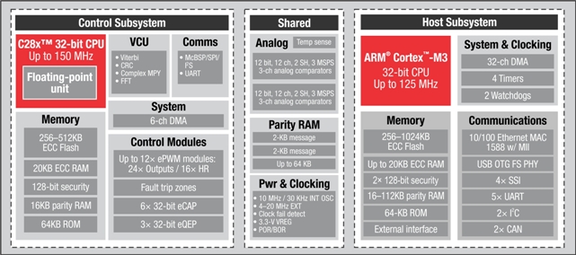
Texas Instruments has developed a family of microcontrollers with TI’s C28x core and control peripherals with an ARM Cortex-M3 core and connectivity in a clearly partitioned architecture that supports real-time control in a single, cost-efficient device. Software libraries for the key applications for the Concerto C2000 MCUs - digital power, motor control and renewable energy -  are due in Q3 this year.
To make them easy to use, the devices are supported by an intuitive software infrastructure as well as application and connectivity libraries within controlSUITE software. The series includes multiple safety and security features and is code compatible across the C2000 platform to enable scalability and code reuse in green applications such as intelligent motor control, renewable energy, smart grid, digital power and electric vehicles.
Greener applications require the performance of a real-time control MCU to execute complex algorithms needed for precise, efficient power conversion, which is the essence of efficient motor control, renewable energy and smart grid technologies. But to take that efficiency to new levels that can dramatically save energy, these applications must also be connected for remote data sharing, diagnostics, monitoring and control. The $7 Concerto MCUs enable developers to do both real-time control and connectivity within one microcontroller, eliminating the traditional need to choose between optimal performance and advanced connectivity.

Features and benefits:
  • Real-time control subsystem based on TI’s C28x core with floating point and the Viterbi Complex Math Unit delivers 13X performance over existing MCUs as well as industry-leading control peripherals required to design the most reliable, efficient green applications
  • Robust host communication subsystem based on Cortex-M3 and connectivity peripherals such as Ethernet, USB On-The-Go, dual CAN, and multiple serial communication ports
  • Performance can be tailored to different applications with options for 150/75 MHz, 100/100 MHz or 60/60 MHz on the C28x and Cortex-M3 cores, respectively
  • Safety and security features, including up to 1 MB of flash and 132 KB RAM with error correction, parity on CAN and interrupt registers, redundancy for functions, and lock protection
  • Free turnkey application and connectivity software libraries, including Ethernet and USB (Digital power, motor control and renewable energy libraries will be available in 3Q11)
  • Speeds design with simple development environment that supports programming each subsystem independently
  • Roadmap for tailored devices to meet specific smart grid applications, such as smart electric meters and concentrators
The new Concerto F28M35x Experimenter Kit includes a F28M35x controlCARD and docking station to enable developers to easily begin evaluation and development. The modular controlCARD is hardware compatible with TI’s C2000 application-specific development kits, and software to further support development on the kits will be available later this year. Free, on-demand training for Concerto MCUs is immediately available online, and is a great way for developers to begin further exploring the optimized architecture, tailored features and easy-to-use software infrastructure of the devices.
Available in a 144 QFP package, Concerto MCUs now start at $6.99 at 1K and samples can be immediately ordered at www.ti.com/concerto-es-lp-pr. The Concerto F28M35x Experimenter Kit is priced at $139. The Concerto F28M35x controlCARD is also available individually for $99. Both are immediately available to order atwww.ti.com/concerto-es-lp. There is an estimated 4 week lead time for samples and kits.


Related articles
Enhanced by Zemanta

World's first production-ready Bluetooth 4.0 low energy heart-rate monitor

Belt will work with any Bluetooth version 4.0 smartphone or gadget
By Nick Flaherty www.flaherty.co.uk


Wireless sports & fitness monitoring developer and manufacturer Dayton Industrial has developed a heart rate chest belt that is ready to go into volume production using a Bluetooth 4.0 chip from Nordic Semiconductor.
Nordic believes this will spur the development of brand new Bluetooth low energy smartphone-based health and fitness monitoring apps and motivational social media data sharing
This means anyone that owns a smartphone with the latest version 4.0 of Bluetooth (that includes Bluetooth low energy as a hallmark feature) will be able to set-up and use a wireless heart-rate (HR) belt within seconds and so spur the development of a whole new range of Bluetooth low energy-based health and fitness apps that could include new ways of collecting, interpreting, and displaying HR training data – including motivational social media-based data and progress sharing.
The belt uses Nordic's nRF8001 RF chip that enables the belt to run for up to 1.5 years from a CR2032 coin cell under typical usage conditions (1-hour per day) while featuring an extremely slim (1.1cm-thick) and compact (3.8 x 6.5 cm) plastic sensor housing that supports a soft fabric finished belt product weighing just 46g (less than the weight of two AA batteries).
"This is not only the first Bluetooth low energy product Dayton Industrial has developed but also the slimmest wireless heart-rate belt we have ever produced," said Johnson Chan, Product Engineering Manager at Dayton. "We have partnered with Nordic Semiconductor for many years and will continue to do so as we roll out further brand new Bluetooth low energy sports & fitness product platforms in the future."
Over half the ULP heart-rate belts shipped globally last year were manufactured by Hong Kong-based Dayton (as measured by sales revenue and according to InMedica, a division of IMS Research).
"Heart rate monitors are one of the first and most sought after use cases for Bluetooth low energy," said Geir Langeland, Nordic Semiconductor's Director of Sales & Marketing. "This Dayton product platform will now sit alongside established ANT+ interoperable HR belt products and other non-interoperable proprietary alternatives, and give consumers an even wider choice when it comes to monitoring their heart rate and so support an even more vibrant HR monitoring market with solutions for everyone."
Bluetooth low energy (now a hallmark of the latest Bluetooth v4.0 specification) has been designed from the outset to extend Bluetooth wireless connectivity to compact, coin cell-powered devices such as sports & fitness monitors. Nordic has been at the forefront of the group that defined the Bluetooth low energy specification since becoming a foundation member of Nokia’s Wibree Alliance in 2006 and the Alliance became part of the Bluetooth Special Interest Group (SIG) in June 2007.
Enhanced by Zemanta

Monday, June 13, 2011

Broadcom develops 1GHz full band cable tuner for fast channel changes

40nm DOCSIS3.0 tuner with full 1GHz bandwidth 
By Nick Flaherty www.flaherty.co.uk

Broadcom has developed a tuner for cable TV systems that spans the whole 1GHz bandwidth, replacing multiple tuners and providing a fast channel change regardless of the frequency.
It has integrated the industry's first 1GHz Full-Band Capture digital tuning technology into three new 40nm hybrid IP cable set-top box (STB) and DOCSIS 3.0 gateway SoC solutions. These deliver the cable tuner density and performance that operators need to convert current cable systems to IP-based video platforms. This provides scalable bandwidth while reducing power, cost and simplifying cable tuner design while accelerating the deployment of DOCSIS 3.0 cable gateways and hybrid IP cable STBs. Hybrid IP cable STBs will more efficiently bring additional video streams and IP services to connected devices in the home ecosystem and are expected to grow at 40 percent through 2014. 
"Driving the next frontier in cable TV, Broadcom's breakthrough in tuner design reduces the cost to transition current cable platforms to hybrid IP-based solutions, proliferating IP content delivery and services throughout the home and to connected devices," said Dan Marotta, Executive Vice President & General Manager, Broadcom's Broadband Communications Group.
The FBC technology directly digitizes the entire 1GHz downstream spectrum, replacing the need for a large number of tuners with only one FBC digital tuner. Full-Band Capture technology advantages include:
  • Digital tuning: engineered with new enhanced signal processing techniques that exceed the most challenging performance requirements demanded by operators.
  • Bandwidth deployment flexibility: any demodulator can tune to any frequency removing wideband "block" tuner restrictions.
  • Reduced power consumption: more than 50 percent reduction with new tuner architecture.
  • Faster channel change: FastRTV channel change technology paired with Full-Band Capture provides quick channel change regardless of frequency.
  • Reduced system cost: dramatically minimizes the number of components by replacing up to nine cable tuners in a system with only one FBC digital tuner supporting as many demodulators as required.
Broadcom's 40nm 8-QAM BCM3128 and 4-QAM BCM3124 cable multi-receiver SoCs and the 400 Mbps BCM3383 Euro/DOCSIS 3.0 cable gateway SoC are the industry's first fully integrated solutions to support FBC technology and are now shipping to customers.
Enhanced by Zemanta

IBM develops 10GHz graphene devices for wireless

Wafer scale integrated circuits running up to 10GHz

By Nick Flaherty www.flaherty.co.uk

IBM researchers have developed the first integrated circuit fabricated from wafer-size graphene, and demonstrated a broadband frequency mixer operating at frequencies up to 10GHz.
Designed for wireless communications, the graphene-based analogue integrated circuit could improve today's wireless devices and points to the potential for a new set of applications. Graphene, the thinnest electronic material consisting of a single layer of carbon atoms packed in a honeycomb structure, possesses outstanding electrical, optical, mechanical and thermal properties that could make it less expensive and use less energy inside portable electronics like smart phones.
The integrated circuit consists of a graphene transistor and a pair of inductors compactly integrated on a silicon carbide (SiC) wafer, overcomes these design hurdles by developing wafer-scale fabrication procedures that maintain the quality of graphene and, at the same time, allow for its integration to other components in a complex circuitry.
"Just a few days before IBM commemorates its 100th anniversary, our scientists have achieved a nanotechnology milestone which continues the company's century-long pursuit of innovation and technology leadership," said T.C. Chen, vice president, Science and Technology, IBM Research. "This research breakthrough has the potential to increase the performance of communication devices that enable people to interact with greater efficiency."
The breakthrough is also a major milestone for the Carbon Electronics for RF Applications (CERA) program, funded by DARPA.
In this demonstration, graphene is synthesized by thermal annealing of SiC wafers to form uniform graphene layers on the surface of SiC. The fabrication of graphene circuits involves four layers of metal and two layers of oxide to form top-gated graphene transistor, on-chip inductors and interconnects.
The circuit operates as a broadband frequency mixer, which produces output signals with mixed frequencies (sum and difference) of the input signals. Mixers are fundamental components of many electronic communication systems. Frequency mixing up to 10 GHz and excellent thermal stability up to 125 degrees C has been demonstrated with the graphene integrated circuit.
The fabrication scheme developed can also be applied to other types of graphene materials, including chemical vapor deposited (CVD) graphene films synthesized on metal films, and are also compatible with optical lithography for reduced cost and throughput.
Previously, the team has demonstrated standalone graphene transistors with a cut-off frequency as high as 100 GHz and 155 GHz for epitaxial and CVD graphene, for a gate length of 240 and 40 nm, respectively.
Enhanced by Zemanta

Intel teaches machines to build their own device drivers

Intel teaches machines to build own device drivers • The Register

TERMITE takes synthesis to the device driver, reducing errors and simplifying ports to new operating systems
Enhanced by Zemanta

General Dynamics to Develop Open Architecture Back-End RF Processor for US Air Force

Finally, a plug-and-play DSP 
By Nick Flaherty www.flaherty.co.uk

The US Air Force has awarded General Dynamics Advanced Information Systems a $7.8m contract to develop an Open System Architecture (OSA) common back-end digital processor for the entire family of Air Force radio frequency (RF) electronic devices, to include radars, SIGINT sensors, electronic-warfare and communication systems.
Under the contract, General Dynamics will use open interface standards to develop modular, "plug and play," multi-mission electronic back-end processors that leverage technologies developed under other OSA initiatives conducted by the Office of Naval Research. Back-end processors are used to analyse sensor signals, once they have been converted from analogue to digital formats, that have been collected by the RF devices.
General Dynamics will provide a single family of processors capable of handling the digital processing needs of all Air Force RF systems. Because the General Dynamics open architecture eliminates the need for proprietary interfaces, the Air Force will benefit from competition from multiple vendors and will be able to take advantage of rapid technology upgrades as well as cost savings throughout the lifecycle of the processor.
Work under the contract will be performed in Bloomington, Minn., Fairfax, Va., Waimea, Hawaii and Ypsilanti, Mich.
"Leveraging our proven open architecture and open business model, General Dynamics will provide the Air Force with an increased airborne and spaceborne processing capability and a significant reduction in life-cycle cost," said Mike Tweed-Kent, vice president and general manager of Mission Integration Systems Division for General Dynamics Advanced Information Systems.
Enhanced by Zemanta