All the latest quantum computer articles

See the latest stories on quantum computing from eeNews Europe

Friday, November 29, 2019

Kontron expands COMe Type 6 boards with AMD Ryzen processors

By Nick Flaherty www.flaherty.co.uk

Kontron is expanding its portfolio of COMe-cVR6 (E2) Computer-on-Modules in the COM Express  Compact Type 6 form factor with new variants of AMD's Ryzen processor.

These will use the Ryzen V1404I with 4x 2.0 GHz and a power consumption of 12 to 25W. Versions with ECC memory down or with DDR4 SO-DIMM socket are possible. Both are designed for the industrial extended temperature range between -40 and +85 degrees Celsius. This makes the COMe-cVR6 modules particularly suitable for use in harsh environmental conditions, such as power utilities or in the defence sector, as well as for applications in medical imaging or industrial image processing, and for complex automation systems. 

The COMe-cVR6 (E2) computer-on-modules are based on the AMD Embedded V1000 processors, and the smaller form factor of the COM Express  Compact Modules allows significantly more space to be saved. This enables developers to produce more compact designs with maximum performance. In addition, the COMe-cVR6 (E2) variants with soldered-on memory are insensitive to vibration and shock. All other components such as voltage dividers, capacitors and controllers have also been chosen in regards to ensuring maximum resistance to environmental influences.

The new COMe-cVR6 (E2) supports the Kontron APPROTECT security solution based on Wibu-Systems CodeMeter. In addition, Kontron APPROTECT licensing also enables new business models such as 'pay-per-use' or time-based trial versions.
The modules are expected to be available during the first quarter of 2020.

www.kontron.com/products/boards-and-standard-form-factors/com-express/com-express-compact/come-cvr6-e2-.html

Friday, November 22, 2019

Global regulators identify mmWave spectrum for 5G services

By Nick Flaherty www.flaherty.co.uk

After a month of 'difficult' negotiations, regulators at the ITU’s World Radio Conference (WRC-19) meeting this week agreed a range of frequency bands for millimetre wave 5G service.

This impacts on the antenna and chipset designs going forwards for mobile handsets, hubs and wireless links for the Internet of Things (IoT) as well as determining the data bandwidth that will be available for services.

Over 10 GHz of spectrum for 5G in the 26, 40, 47 and 66 GHz ranges was agreed.

"GSA members have participated in the difficult negotiations that have taken place in the run up to this decision, particularly with regards to 26 GHz, keeping in mind the need to protect satellite services in the adjacent spectrum while remaining committed to delivery of high–performance economical solutions to the global markets," said the Global mobile Suppliers Association (GSA).

"The GSA is also delighted that administrations have agreed to study additional spectrum opportunities in the mid-band frequencies between 3.3 and 10.5 GHz, as well as spectrum below 1 GHz. This will help enable 5G services to be further deployed in wider geographical areas, including rural areas, as well as meet the anticipated increased traffic needs of population centres in the next decade."

“The Industry forecast is that by 2024 over 130 Exabytes of data will be transmitted globally every month and the mobile industry will need to massively deploy 5G technology in a broad range of frequency bands to meet this demand," said Joe Barrett, President of the GSA. "Applications that will drive this massive data usage include 8k mobile video, Augmented and Virtual Reality, HD video, industrial automation and robotics, drone and aeronautical networks and the IoT. 

"Spectrum regulators have recognized that low-, mid- and high-band frequencies need to be available and harmonised globally as much as is possible to ensure mobile broadband can meet the expanding services both industry and consumers are expecting in the coming years," he said.

There are 183 5G devices from 72 vendors tracked in the GSA GAMBoD database, with at least 42 are commercially available: https://gsacom.com/paper/5g-device-ecosystem-november-2019/

There are now 50 5G commercial networks in 27 countries. By the end of October 2019, 328 operators in 109 countries had announced they were investing in 5G: https://gsacom.com/paper/50-5g-commercial-networks-november-snapshot/

5G Modems Chipsets + LTE & IoT: Status Update: https://gsacom.com/paper/5g-modems-chipsets-status-update-2/

Thursday, November 21, 2019

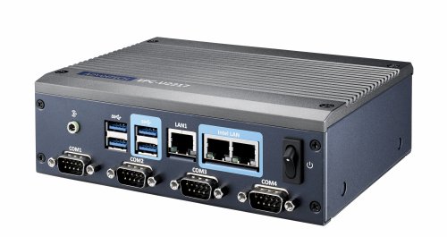
Advantech launches palm-sized PC with Atom 3900 for IoT

By Nick Flaherty www.flaherty.co.uk

Advantech has launched a palm-sized embedded controller measuring 170 x 117 x 52.6mm based on the latest Intel Atom E3900 processor technology to give a 30% CPU performance enhancement and a 45% graphic performance boost. It is also certified for use with the AWS Greengrass and Microsoft Azure IoT Edge cloud services for the Internet of Things.


The EPC-U2117 is designed with dual display output, multiple I/O, and 12 to 24V DC power inputs, which target smart vending machines, digital signage, smart kiosk, and more. 

It runs Microsoft Windows 10 IoT Enterprise and Linux OS as well as Advantech’s WISE-PaaS DeviceOn intelligent software integrated for remote system monitoring and management that also BIOS/FW OTA updates to upgrade the system and devices with latest firmware to keep everything running at peak performance.

THe unit can be mouted as a desktop PC, or via wall, or DIN-Rail mount. The top extruded aluminium passive heatsink thermal solution is designed for -20 ~60 °C wide temperature operation and there are integrates two expansion slots including one M.2 for Wi-Fi or GPU module, and one full size Mini PCIe for 3G/LTE connection or mSATA storage. 

The EPC-U2117 supports multiple storage, which includes onboard eMMC up to 128GB, mSATA, and 2.5” SSD/HDD for flexible storage options. Customers can install OS and key data in eMMC for best security protection and reliability. If customer request big storage capacity and high data transfer, they can use mSATA or SATA SSD for better storage performance.


Monday, November 18, 2019

Infineon teams with Klika Tech on smart buildings

By Nick Flaherty www.flaherty.co.uk

Infineon Technologies has teamed up with Klika Tech to connect smart buildings to the cloud. The partnership brings together Infineon’s chips with Klika Tech's Cloud technology based on Amazon Web Services (AWS).

“Klika Tech is a strong addition to Infineon’s partner network, offering complementary capabilities to develop innovative solutions for smart building applications,” said Oliver Henning, Head of Partnership Management & Emerging Application Business at Infineon’s Power Management & Multimarket division. “

Klika Tech is a global developer of end-to-end networks in the Internet of Things (IoT) using cloud-based services. It is using Infineon's chips for product development, as well as rapid development kits with full AWS cloud integrations. The companies are focusing on end-to-end solutions across applications such as smart building, smart city, smart home, connected devices as well as autonomous and electric cars.

“Collaborations among hardware, software and services providers are the genesis of the custom IoT and Cloud solutions that are enabling companies to reduce their development efforts and expedite time to market. This holds especially true for smart building and smart home applications.” said Gennadiy M. Borisov, President and Co-CEO at Klika Tech. “We look forward to building on our relationship with Infineon and the integration of their outstanding sensor portfolio with AWS services.”

Cloud-based Machine Learning (ML) algorithms provide predictive maintenance capabilities for current equipment condition analysis, informs maintenance personnel, and can trigger specific tasks to keep machines running at optimum levels. Implementing a predictive maintenance plan can detect improper installation, make equipment more energy efficient, predict costly failures, and extend equipment life to reduce total costs of ownership.

www.klika-tech.com

Packet-based power ... Teslas's Berlin plans ... Battery minerals from deep sea nodules ... Power supply for immersed computing

Power news at eeNews Europe Power by Nick Flaherty www.flaherty.co.uk

. VoltServer raises $7.4m for packet-based power

. Tesla gigafactory will boost electric vehicle cluster in Berlin


. Infineon optimistic despite a poor year ahead

POWER TECH TO WATCH

. Trial shows network monitoring for UK grid

. Deep sea nodule mining project to harvest battery elements

. Passive cooling boost from silica microspheres

NEW POWER PRODUCTS

. First AC-DC supply for immersed computing


. Heat sinks for high power devices


. 2.4MHz DC-DC buck regulator has low quiescent power

TECHNICAL PAPERS

. Selecting the Best Inductor for Your DC-DC Converter

. Designing for ultra-low power applications through empirical methods

Friday, November 15, 2019

First dual Arm Cortex-M33 wireless chip for low power IoT applications

By Nick Flaherty www.flaherty.co.uk

Nordic Semiconductor has developed a flexible dual-processor hardware architecture and advanced security features for complex IoT applications using two ARM Cortex-M33 cores.

The nRF5340 combines a high performance application processor with a fully programmable, ultra low power network processor, plus advanced root-of-trust and trusted execution security features, into a low power multiprotocol SoC ready for professional lighting, industrial automation, advanced wearables, and other complex IoT applications

This is the first in the nRF53 family, building on the nRF51 and nRF52 Series multiprotocol SoCs. The nRF5340 supports major RF protocols including Bluetooth 5.1/Bluetooth Low Energy (Bluetooth LE), Bluetooth mesh, Thread, and Zigbee.

The nRF5340 SoC is designed for extended operating temperature up to 105°C, which together with its multiprotocol support and advanced security features makes it suited for professional lighting and industrial applications as well as wearables.

The QSPI peripheral is augmented to interface with external memory at 96 MHz, and a 32 MHz High Speed SPI peripheral is integrated to interface with displays and complex sensors.

The chip incorporates Arm CryptoCell-312, Arm TrustZone technology, and Secure Key Storage for the highest level of security. With Arm CryptoCell-312 the most common Internet encryption standards are hardware accelerated and Arm TrustZone provides system-wide hardware isolation for trusted software by creating secure and non-secure code execution areas on a single core. The nRF5340’s combined security features enable advanced root-of-trust and secure firmware updates while protecting the SoC from malicious attack.

The nRF5340 is based around dual Arm Cortex-M33 processors; a high performance application processor running up to 128 MHz (510 CoreMark) with dedicated 1 MB Flash and 512 KB RAM, and a fully programmable, ultra low power network processor running at 64 MHz (238 CoreMark) with dedicated 256 KB Flash and 64 KB RAM. 

The application processor is optimised for power efficiency at 65 CoreMark/mA, has an 8 KB 2-way associative cache, is DSP and floating point capable and offers voltage and frequency scaling options. The application processor integrates the Arm Cryptocell-312, Arm TrustZone, and Secure Key Storage advanced security features, plus a wide range of interface peripherals including NFC, USB, QSPI, and High Speed SPI. 

The M33 network processor is even more efficient at 101 CoreMark/mA and is optimised for low power during radio operation and low duty-cycle sensor data collection. Programmable access to the network processor offers optimal implementation of proprietary 2.4 GHz protocols, ensuring portability from the nRF51 and nRF52 Series.

The nRF5340 incorporates a new, power-optimized multiprotocol 2.4 GHz radio with a TX current of 3.2 mA (0 dBm TX power, 3 V, DC/DC) and RX current of 2.6 mA (3 V, DC/DC). Sleep current is as low as 1.1 µA. The SoC features enhanced dynamic multiprotocol support enabling concurrent Bluetooth LE and Bluetooth mesh/Thread/Zigbee operation for provisioning/commissioning and interaction with a mesh network from a smartphone using Bluetooth LE. The radio is capable of all Bluetooth 5.1 Direction Finding features. The nRF5340 operates over a 1.7 to 5.5 V supply voltage range, allowing supply from rechargeable batteries and USB. The SoC integrates XTAL load capacitors for both 32 MHz and 32.762 kHz crystals, lowering by four the number of external components required compared with Nordic’s nRF52 Series - reducing both bill-of-materials (BOM) and solution size.

The software development kit integrates the Zephyr RTOS, a Bluetooth LE protocol stack, application examples, and hardware drivers. It unifies low power cellular IoT and low power, short range wireless development and is publicly hosted on GitHub, offers source code management with Git and comes with free SEGGER Embedded Studio IDE support. 

Nordic has also launched the nRF5340 PDK, an affordable, single board preview development kit for the nRF5340. The nRF5340 PDK makes all of the nRF5340’s features and GPIOs available to the developer and comes with an on-board SEGGER J-Link debugger for programming and debugging the SoC.

“Bluetooth, Thread, Zigbee and other low power wireless technologies now form a critical part of the IoT. Developers are already working on tomorrow’s commercial products based on highly-complex applications such as property tech, location services, medical, smart home, and Industrial IoT. These demand greater computational power with high security, yet developers expect Nordic’s wireless solutions to remain compact and highly energy-efficient,” says Kjetil Holstad, Director of Product Management at Nordic Semiconductor.

“The nRF5340 SoC is designed to meet these needs and more. The product is the culmination of Nordic’s decades of experience in ultra low power wireless, the lessons learned from the development and support of the nRF51 and nRF52 Series over the last seven years, and several years of focused product development from perhaps the most experienced low power wireless R&D team in the world. The nRF5340 and nRF Connect SDK combine to make it easy for developers to build wireless applications that until now were impossible.”

The nRF5340 PDK is available now through Nordic’s distribution network. nRF5340 SoC engineering samples will be available soon in a 7x7 mm aQFN package with 48 GPIOs.

AI chip reaches 1petaOps/s

By Nick Flaherty www.flaherty.co.uk

US startup Groq has developed a single chip for machine learning that is capable of 1 PetaOp/s performance.

The architecture is also capable of up to 250 trillion floating-point operations per second (FLOPS) and has been used to create the Tensor Streaming Processor shown on this PCIe board which is currently being tested by customers

“We are excited for the industry and our customers,” said Jonathan Ross, Groq’s co-founder and CEO. “Top GPU companies have been telling customers that they’d hoped to be able to deliver one PetaOp/s performance within the next few years; Groq is announcing it today, and in doing so setting a new performance standard. The Groq architecture is many multiples faster than anything else available for inference, in terms of both low latency and inferences per second. Our customer interactions confirm that. We had first silicon back, first-day power-on, programs running in the first week, sampled to partners and customers in under six weeks, with A0 silicon going into production.”

The architecture provides both compute flexibility and massive parallelism without the synchronization overhead of traditional GPU and CPU architectures. Groq’s architecture can support both traditional and new machine learning models, and is currently in operation on customer sites in both x86 and non-x86 systems.

Groq’s new, simpler processing architecture is designed specifically for the performance requirements of computer vision, machine learning and other AI-related workloads. Execution planning happens in software, freeing up valuable silicon real estate otherwise dedicated to dynamic instruction execution. The tight control provided by this architecture provides deterministic processing that is especially valuable for applications where safety and accuracy are paramount. 

Compared to complex traditional architectures based on CPUs, GPUs and FPGAs, Groq’s chip also streamlines qualification and deployment, enabling customers to simply and quickly implement scalable, high performance-per-watt systems.

“Groq’s solution is ideal for deep learning inference processing for a wide range of applications,” said Dennis Abts, Chief Architect at Groq, “but even beyond that massive opportunity, the Groq solution is designed for a broad class of workloads. Its performance, coupled with its simplicity, makes it an ideal platform for any high-performance, data- or compute-intensive workload.”

This is similar to the architecture launched by Blaize earlier this week, with a focus on software planning and a simpler chip - see AI CHIP STARTUP TAPS TWO UK DESIGN TEAMS

www.groq.com

Wednesday, November 13, 2019

PICMG finalises pin out for high performance COM modules

By Nick Flaherty www.flaherty.co.uk

The PICMG COM-HPC technical subcommittee approved the pinout of the new high-performance Computer-on-Module specification. 

The COM-HPC standard is now entering the home stretch for the ratification of version 1.0 of the specification, which is scheduled for the first half of 2020. Computer-on-Module manufacturers and carrier board designers who are active in the COM-HPC workgroup can now embark on first edge computing designs based on this pre-approved data, with the expectation to bring them to market in time with the launch of new high-end embedded processor generations from Intel and AMD next year.
"Within PICMG we are currently working on the next generation Computer-On-Module standard which is of utter importance for the embedded and edge computing world," said PICMG president Jessica Isquith. "Next to the physical footprint, the pinout is the most essential milestone. It could only be pre-approved so quickly because we managed to get all key market players, including semiconductor manufacturers such as Intel, around one table in the COM-HPC technical subcommittee, thereby also making sure that the standard will be the best fit possible for future processor generations.

"A new Computer-on-Module specification is a complex task that involves many stakeholders," said committee chairman Christian Eder, who says he is confident that the specification can be officially ratified before the next high-end embedded processors hit the market: 

"We officially started our work back in October 2018 and are on schedule to release new COM-HPC modules, carrier boards and solution platforms in time with the next high-end embedded processor generations. They will extend the existing PICMG COM Express module standards with new solutions that move in the direction of headless edge server and more multifunctional edge client solutions," he said.

With the adoption of the pinout, all committee members now have a solid working basis from which to offer interfaces supporting up to 100 GbE and PCIe Gen 4.0 and Gen 5.0 as well as up to eight DIMM sockets and high-speed processors with more than 200 watts on standardized COM-HPC modules, and to work on standard-compliant carrier board designs.

Members of the PICMG COM-HPC committee include the University of Bielefeld and Adlink, Advantech, Amphenol, AMI, congatec, Elma Electronic, Emerson Machine Automation Solutions, ept, Fastwel, GE Automation, HEITEC, Intel, Kontron, MEN, MSC Technologies, N.A.T., Samtec, SECO, TE Connectivity, Trenz Electronic and VersaLogic. Adlink, congatec and Kontron are also committee sponsors. e.

More information on the COM-HPC Computer-on-Module standard and its pinout is at www.congatec.com/COM-HPC

Thursday, November 07, 2019

COM Express Type 7 module for embedded low power server

By Nick Flaherty www.flaherty.co.uk

D
Kontron has launched a smaller version of its COMe-bDV7 (COM Express basic), for use in extremely space-constraint and low-power, fanless embedded applications. 

The COMe-cDV7 module carries a member of the Intel Atom C3000 processor family with up to 16 cores and two SODIMM sockets for up to 2x 32GB DDR4 memory (ECC) offering a balanced core count vs memory size implementation. 

Available interfaces are up to 14x PCI Express Gen 3.0 lanes, up to 3x USB 3.0, 2x SATA Gen3, 2x UARTs and optionally support of eMMC 5.1. In combination with up to four 10GbE-KR ports, the COMe-cDV7 is aimed at network intensive implementations, such as real-time Industry 4.0 edge servers, micro servers, network appliances, robotics or energy. 

The KR design allows for maximum flexibility by defining the physical interface – KR for backplane connectivity, copper (RJ45) or fibre (SFP+) on the base board. Furthermore the available NC-SI signals allow the connection of a Baseboard Management Controller (BMC) on the baseboard for the purpose of enabling out-of-band remote manageability. This enhances reliability and helps reduce the overall operating cost in general.

In addition, the COMe-cDV7 module supports the Kontron APPROTECT security solution based on Wibu-Systems CodeMeter. Kontron APPROTECT Licensing also enables new business models such as 'pay-per-use' and time-based trial versions.

The module is available immediately including Board Support Packages for Linux and Windows Server 2012 R2, 2016 and also in industrial-grade versions.

www.kontron.de/products/boards-and-standard-form-factors/com-express/com-express-basic/come-bdv7.html


Tuesday, November 05, 2019

3D printing embeds silver nanowires

By Nick Flaherty www.flaherty.co.uk

Researchers at Rutgers University in the US have embedded high performance electrical circuits inside 3D-printed plastics, which could lead to smaller and versatile unmanned aircraft and better-performing small satellites, biomedical implants and smart structures.

They used pulses of high-energy light to fuse silver nanowires, resulting in circuits that conduct ten times more electricity than the state of the art, according to a study in the journal Additive Manufacturing. This higher conductivity reduces energy use, extend the life of devices and increase their performance.

“Our innovation shows considerable promise for developing an integrated unit – using 3D printing and intense pulses of light to fuse silver nanoparticles – for electronics,” said Rajiv Malhotra, an assistant professor in the Department of Mechanical and Aerospace Engineering in the School of Engineering at Rutgers University–New Brunswick.

Embedding electrical interconnections inside 3D-printed structures made of polymers, or plastics, can create new paradigms for devices that are smaller and more energy-efficient. Such devices could include CubeSats, drones, transmitters, light and motion sensors and Global Positioning Systems. Such interconnections are also often used in antennas, pressure sensors, electrical coils and electrical grids for electromagnetic shielding.

The team used intense pulsed light sintering with high-energy light from a xenon lamp to fuse long thin rods of silver as nanowires in the 3D printed objects. The next steps include making fully 3D internal circuits, enhancing their conductivity and creating flexible internal circuits inside flexible 3D structures, said Malhotra.

Friday, November 01, 2019

Renesas consolidates its energy harvesting controller family

By Nick Flaherty www.flaherty.co.uk

Renesas Electronics has consolidated its energy harvesting embedded controllers into a single family.

The RE Family is based on Renesas’ proprietary SOTB (Silicon on Thin Buried Oxide) process technology, which dramatically reduces power consumption in both the active and standby states, eliminating the need for battery replacement or recharging.

An evaluation kit for the first of the family, the RE01 (formerly the R7F0E embedded controllers), was launched this week to jump start system evaluations for energy harvesting applications.

The RE01 embedded controllers are based on the Arm Cortex-M0+ core, which can operate at clock frequencies up to 64 MHz, and provide up to 1.5 MB of low-power flash memory and 256 KB of SRAM. The RE01 can operate at voltages as low as 1.62 V and the lineup includes three package versions: a 156-pin WLBGA package, a 144-pin LQFP package, and a 100-pin LQFP package. The RE01 also includes an energy harvesting control circuit, an ultra-low power 14-bit A to D converter, and a low power circuit that can rotate, enlarge, or invert graphics data.

"Energy harvesting eliminates the labour and costs associated with battery maintenance and is a key solution contributing to environmental conservation," said Hiroto Nitta, Senior Vice President, Head of SoC Business, IoT and Infrastructure Business Unit at Renesas. "I am extremely pleased that Renesas’ technology innovation with SOTB has enabled these alternative energy solutions, and with the new RE01 Evaluation Kit, Renesas will be making it possible for engineers around the world to quickly start the evaluation. We hope this will accelerate the spread of IoT equipment powered by energy harvesting."

The RE01 Evaluation Kit includes an evaluation board which features an RE01 embedded controller, an interface for the energy harvesting device and a rechargeable battery interface. The Kit also includes an Arduino-compatible interface for easy expansion and evaluation of sensor boards and a Pmod connector to expand and evaluate wireless functionality. 

There is also an ultra-low power LCD expansion board so that users can evaluate display functions faster. The Kit also contains sample code and application notes that serve as references for power management design that eliminates the need for battery maintenance, and driver software that supports CMSIS, Arm’s Cortex Microcontroller Software Interface Standard. 

Sample code for ultra-low power A/D converters, digital filter and FFT (fast Fourier transform) routines, 2D graphics MIP LCD displays, and secure boot and secure firmware update functions for improved security are available. With these features, this kit makes it possible to adopt energy harvesting based on RE01 Group devices at the system level and will accelerate the development of equipment that does not require battery maintenance.

The kit uses the IAR Embedded Workbench for Arm which can use the high efficiency IAR C/C++ compiler, and e2 studio (note 2) which can use the free GNU compiler are available as the developmental environment.

These embedded controllers make it possible for applications to perform highly accurate sensing and data judgement by excluding noise from signal data when they are used as biological monitors or outdoor environmental sensing applications. By eliminating the need for battery maintenance in a wide range of applications, these embedded controllers will contribute to the increasingly widespread use of IoT equipment, such as wearable equipment without the inconvenience of recharging batteries, and sensing applications for homes, buildings, factories and farms, where manual changing or recharging of batteries is difficult.

Renesas will continue expanding the RE Family beyond 2020 with new members including small memory sizes featuring up to 256 KB of flash memory.

www.renesas.com/products/microcontrollers-microprocessors/re.html
www.renesas.com/products/software-tools/boards-and-kits/eval-kits/evaluation-kit-re01-1500kb.html