All the latest quantum computer articles

See the latest stories on quantum computing from eeNews Europe
Showing posts with label optical computing. Show all posts

Wednesday, December 29, 2010

Five reasons why we won't see IBM's holographic display in five years - video

By Nick Flaherty www.flaherty.co.uk


IBM has released its prediction of five key technologies for the next five years, and on the whole they are pretty sound: fuel cell batteries are here and making headway in a number of markets, the smart grid will take existing technologies and apply them to wide area power systems, sensors will be everywhere (absolutely!) and smart algorithms can take the pain out of commuting - so far, so good. But the one that IBM has chosen to headline is holographic phone calls (and mobile ones at that).

IBM says:
In the next five years, 3-D interfaces – like those in the movies – will let you interact with 3-D holograms of your friends in real time. Movies and TVs are already moving to 3-D, and as 3-D and holographic cameras get more sophisticated and miniaturized to fit into cell phones, you will be able to interact with photos, browse the Web and chat with your friends in entirely new ways.

Scientists are working to improve video chat to become holography chat - or "3-D telepresence." The technique uses light beams scattered from objects and reconstructs a picture of that object, a similar technique to the one human eyes use to visualize our surroundings.

This is nonsense for a number of reasons:

  1. Photonics doesn't scale. We haven't been able to make photonics scale like silicon - researchers have been trying for 20 years to make the photonic computer, and are still trying. It will take more than 5 years to make commercial, large scale photonic technology small enough for the home, let alone the mobile
  2. Photonics won't be cheap enough. As it doesn't scale, it's also going to be hard to make it cheap enough. There are LED projectors now but there's some large steps to take to make this a consumer product
  3. It's too power hungry for mobile. And not low cost enough. Or small enough. It won't make the home, let alone the mobile.
  4. Video calling is only just taking off. It has taken 20 years for the idea of 2D video calling to take off. A lack of standards and a social resistance is only just being overcome with Skype in the office (not in the living room even now) and Facetime on the Apple 4. There is still a lot of resistance to installing a projector in the home that will take a lot to overcome. 
  5. It's the face, stupid. Apple is driving video calling through the face - being able to see the other person's expression. That's not what the 3D system provides. 
That's not to say it won't be incredibly useful, just not in the home. The key is that the engineers at IBM Research are working on new ways to visualize 3-D data, working on technology that would allow engineers to step inside designs of everything from buildings to software programs, running simulations of how diseases spread across interactive 3-D globes, and visualizing trends happening around the world on Twitter – all in real time and with little to no distortion. 
This is where the technology will take off, where size, cost and power are less important than visualising large amounts of data. From there it make its way into the home office with new projectors, but this will take more than five years to happen.


Related articles


Enhanced by Zemanta

Tuesday, March 23, 2010

World's smallest microcavity laser for optical computing

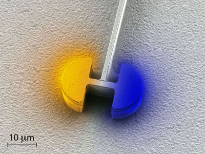
From Nanowerk, physicists at ETH-Zurich have developed the smallest electricallyumped laser in the world that could revolutionize chip technology ("Microcavity Laser Oscillating in a Circuit-Based Resonator").

The laser is 30 micrometers long, eight micrometers high and has a wavelength of 200 micrometers. This makes the laser considerably smaller than the wavelength of the light it emits – difficult, as lasers normally can’t be smaller than their wavelength! So instead of using a resonant cavity, the researchers used an electrical resonant circuit made up of an inductor and two capacitors where the light is effectively “captured” in it and induced into self-sustaining electromagnetic oscillations on the spot using an optical amplifier.

This means the size of the resonator is no longer limited by the wavelength of the light and can in principle be scaled down to any size. This makes the microlaser very interesting for chip manufacturers as an optic alternative to the transistors. “If we manage to approximate the transistors in terms of size using the microlasers, one day they could be used to build electro-optic chips with an extremely high concentration of electronic and optic components”, says researcher Christoph Walther.

Reblog this post [with Zemanta]

Tuesday, March 09, 2010

IBM looks to optical computing with nanophotonic avalanche detector

IBM scientists have unveiled a significant step towards replacing electrical signals that communicate via copper wires between computer chips with tiny silicon circuits that communicate using pulses of light. As reported in the recent issue of the scientific journal Nature, this is an important advancement in changing the way computer chips talk to each other. 
The device, called a nanophotonic avalanche photodetector, is the fastest of its kind and could enable breakthroughs in energy-efficient optical computing.
The IBM device uses the “avalanche effect” in Germanium, a material currently used in production of microprocessor chips. Conventional avalanche photodetectors are not able to detect fast optical signals because the avalanche builds slowly.
“This invention brings the vision of on-chip optical interconnections much closer to reality,” said Dr. T.C. Chen, vice president, Science and Technology, IBM Research. “With optical communications embedded into the processor chips, the prospect of building power-efficient computer systems with performance at the Exaflop level might not be a very distant future.”
The avalanche photodetector demonstrated by IBM is the world’s fastest device of its kind. It can receive optical information signals at 40Gbps (billion bits per second) and simultaneously multiply them tenfold. Moreover, the device operates with just a 1.5V voltage supply, 20 times smaller than previous demonstrations. Thus many of these tiny communication devices could potentially be powered by just a small AA-size battery, while traditional avalanche photodetectors require 20-30V power supplies.
“This dramatic improvement in performance is the result of manipulating the optical and electrical properties at the scale of just a few tens of atoms to achieve performance well beyond accepted boundaries,” said Dr. Assefa, the lead author on the paper. “These tiny devices are capable of detecting very weak pulses of light and amplifying them with unprecedented bandwidth and minimal addition of unwanted noise.”
In IBM’s device, the avalanche multiplication takes place within just a few tens of nanometers (one-thousandths of a millimeter) and that happens very fast. The tiny size also means that multiplication noise is suppressed by 50% - 70% with respect to conventional avalanche photodetectors. The IBM device is made of Silicon and Germanium, the materials already widely used in production of microprocessor chips. Moreover it is made with standard processes used in chip manufacturing. Thus, thousands of these devices can be built side-by-side with silicon transistors for high-bandwidth on-chip optical communications.
The Avalanche Photodetector achievement, which is the last in a series of prior reports from IBM Research, is the last piece of the puzzle that completes the development of the “nanophotonics toolbox” of devices necessary to build the on-chip interconnects.
In December 2006, IBM scientists demonstrated silicon nanophotonic delay line that was used to buffer over a byte of information encoded in optical pulses - a requirement for building optical buffers for on-chip optical communications.
In December 2007, IBM scientists announced the development of an ultra-compact silicon electro-optic modulator, which converts electrical signals into the light pulses, a prerequisite for enabling on-chip optical communications.
In March 2008, IBM scientists announced the world’s tiniest nanophotonic switch for “directing traffic” in on-chip optical communications, ensuring that optical messages can be efficiently routed .
The report of this work, entitled “Reinventing Germanium Avalanche Photodetector for Nanophotonic On-chip Optical Interconnects,” by Solomon Assefa, Fengnian Xia, and Yurii Vlasov of IBM’s T.J. Watson Research Center in Yorktown Heights, N.Y. is published in the March 2010 issue of the scientific journal Nature.
IBM has a long history of pioneering advanced silicon technologies to help enhance performance, while reducing size and power consumption. Such advances include the development of the world’s first copper-based microprocessor; silicon-on-insulator (SOI), a technology that reduces power consumption and increases performance by helping insulate the millions of transistors on a chip; and strained silicon, a technology that “stretches”  material inside the silicon decreasing the resistance and speeding the flow of electrons through transistors.

Reblog this post [with Zemanta]