All the latest quantum computer articles

See the latest stories on quantum computing from eeNews Europe

Tuesday, June 14, 2016

Weightless and ETSI partner on low cost wireless standards for IoT

By Nick Flaherty www.flaherty.co.uk

One of the promising narrowband wireless protocols for the Internet of Things, Weightless, is moving towards an international standard.

The Weightless SIG is partnering with the European Telecommunications Standards Institute (ETSI), and a key ultra narrow-band (UNB) LPWAN technology and applications provider, Telensa, is to the board of the Weightless SIG.

In a move widely acknowledged to bring much needed consolidation to the LPWAN space the Weightless SIG will immediately offer its Weightless-N standards activities into the ETSI LTN initiative within TG28, ensuring that all those interested in UNB solutions are represented in a single forum.
This is the first step on standardisation and the move is supported by several other UNB technology companies (announcements to come). Weightless is supported by Neul which in September 2014 was acquired by Huawei.

ETSI is a globally accepted standards development organisation within which the Low Throughput Network (LTN) initiative is developing a standard for LPWAN. This initiative is supported by a number of significant companies including Telensa and Sigfox. ETSI LTN is concentrating on a UNB standard.

There are only two standards bodies that have developed IoT specific standards for unlicensed spectrum based on UNB technology – ETSI and the Weightless SIG.

“In order to reduce fragmentation and enable critical mass in the marketplace we are bringing these two initiatives together, immediately reducing fragmentation and providing a platform around which industry can coalesce,” said Weightless CEO, Professor William Webb. 

Telensa's vertical smart city solutions include smart street lighting, where it now has a footprint of over 1 million lights across the world. Telensa's solutions are based on its own 2-way UNB technology, which it has been progressing to a standard with ETSI for the past 2 years.

"Proprietary ecosystems are no substitute for credible open standards when real market velocity is required, said Will Gibson, CEO of Telensa. "That's why we're delighted to be extending our ETSI standards work by joining the board of Weightless. This partnership signals a growing maturity in the LPWA market and will liberate a new wave of smart city sensor and application developers.”

Low Power Wide Area networks are set to become an integral building block for a variety of connected products and services. Deploying such networks also in unlicensed spectrum is critical to ensuring that the market for IoT connectivity will remain sufficiently competitive. The initiative is important, because it can open up a whole new level of scale benefits to players that are driving the unlicensed networks forward.

Weightless will focus on certification, the eco-system development, marketing and information dissemination and other relevant activities to aid the widespread success of the ETSI standards. It is part of a series of moves by the Weightless SIG to bring consolidation and order to the IoT connectivity technology space.


weightless.org
telensa.com

Open source hypervisor port to MIPS processors brings more security to the IoT

By Nick Flaherty www.flaherty.co.uk

German software developer Kernkonzept has ported the open source L4Re hypervisor to the OmniShield ready MIPS CPUs from Imagination Technologies in a bid to mke IoT applicatiins more secure.

The small footprint L4Re hypervisor, maintained by Kernkonzept, can take advantage of the hardware virtualization technology in MIPS CPUs for more efficient context switching and better use of CPU cycles, leading to improved application headroom and security.

Hardware virtualization is quickly gaining attention beyond its traditional home in the data-center for the benefits it provides across numerous application areas from IoT to consumer to automotive to industrial and beyond. With this technology, connected devices can be designed with numerous distinct domains in which multiple operating systems and applications can run independently at the same time on a single platform.

The L4Re operating system is an open-source system framework for building applications with real-time, security, safety, and virtualization requirements, and the latest update includes a new portable virtual machine monitor called ‘uvmm’ with support for both MIPS and ARM virtualization technology

The OS is built on the principle of a minimal Trusted Computing Base: minimising an application’s attack area by modularization and by reducing its dependencies. It consists of the L4Re hypervisor/microkernel, user-level infrastructure for building trusted native L4Re microapps, and virtual-machine support for running various standard OSes in isolated compartments.

The MIPS OmniShield technology uses the hardware virtualization in the CPU to create multiple domains on a single SoC and this allows the L4Re operating system to consolidate multiple applications with differing security, safety, or real-time requirements. This means multiple isolated tenants or guests can run on the same host, authorizing access to on-chip resources, prioritizing use of shared resources, allocating and managing service interrupts from external sources and peripherals.

“As Imagination continues to expand its MIPS ecosystem and OmniShield security offerings, we are delighted to work with Kernkonzept to bring the proven, highly efficient L4Re hypervisor to MIPS. Open source technologies like L4Re, where entire communities are responsible for developing and maintaining the code, can lead to inherently more reliable systems. We’re seeing a great deal of interest in L4Re for MIPS,” said Jim Nicholas, EVP MIPS Processor IP at Imagination.

Kernkonzept develops the open-source L4Re operating systems and hypervisor for security/safety-critical and virtualization-enabled applications. The Dresden, Germany-based company provides software services for the security-sensitive, real-time, and embedded markets.

“The collaboration is enabling us to take the L4Re operating system into new areas. This technology is already quite strong in areas including government and military. Now it’s making its way into embedded markets such as Wi-Fi routers, cable set-top boxes, home gateways, and automotive where MIPS CPUs have a strong presence,” said  Michael Hohmuth, CEO of Kernkonzept.

The open source prpl Foundation has created a demonstration vehicle that enables companies to see and try out the capabilities of hardware virtualization for themselves. It illustrates the power of a separation-based architecture in providing reliability and ease-of development for next-generation connected devices.

The demonstration builds on prpl’s proof-of-concept demonstration earlier this year of its prplSecurity framework—a comprehensive collection of open source APIs providing hardware-level security controls. That was one of the first public demonstrations of hardware enforced multi-tenant OpenWrt, the Linux distribution at the heart of most of the world’s home gateways.

The new demonstration features several domains including two instances of OpenWrt – one that isolates the Wi-Fi radio, and another that enables access to networking devices. With evolving Wi-Fi channel and frequency regulations, it’s important to ensure the radio is completely isolated, while letting users update their OS and install their own applications on the system. Additional domains can be used for provisioning of third party services such as those from operators and service providers.

The L4Re hypervisor for MIPS is available now at www.kernkonzept.com/download.html. Kernkonzept also provides a supported version of the L4Re hypervisor. 

Monday, June 13, 2016

Programmable Drag-and-drop analogue chip for multiple sensors in the IoT

By Nick Flaherty www.flaherty.co.uk

Cypress Semiconductor has launched a new programmable system-on-chip that simplifies the design of next-generation industrial, home appliance and consumer systems that require multiple sensors. 

Many Internet of Things (IoT) applications require multiple sensors and can benefit from dedicated coprocessors that offload sensor processing from the host and reduce overall system power consumption. At the same time the analogue element of the design is often a challenge. The new PSoC Analogue Coprocessor integrates programmable analogue blocks, including a new Universal Analogue Block (UAB), which can be configured with GUI-based software components. 

Based on a 32-bit ARM Cortex-M0+ signal processing engine, it delivers a fully programmable analog front end with op amps, programmable gain amplifiers, analog multiplexers, analog-to-digital converters, analogue filters and digital-to-analogue converters (DACs). This simplifies the design of custom analogue front ends for sensor interfaces by allowing engineers to update sensor features quickly with no hardware or host processor software changes, while also reducing overall costs.

For example, in home automation applications, engineers can easily configure the coprocessor to continuously monitor multiple sensors, such as temperature, humidity, ambient light, motion and sound, allowing the host to stay in a standby low-power mode. Future design changes to support new sensor types can also be easily implemented by reconfiguring the programmable analog blocks. 

The design of custom sensor interfaces is handled by Cypress’s free PSoC Creator Integrated Design Environment (IDE), which simplifies system design by enabling concurrent hardware and firmware development using PSoC Components—free embedded ICs represented by an icon in the IDE. Engineers can easily configure the programmable analog blocks in the Analogue Coprocessor by dragging and dropping components on the PSoC Creator schematic and customizing them with graphical component configuration tools. The components offer fully engineered embedded initialization, calibration and temperature correction algorithms.

“The PSoC Analogue Coprocessor makes sensor interface design accessible to embedded systems engineers without requiring expertise in analog system design; this comes with the added benefit of enabling rapid prototyping and design iterations in software with no hardware changes by simply modifying components in PSoC Creator,” said John Weil, vice president of MCU marketing at Cypress. “Cypress has pioneered and perfected programmable analog technology for 15 years, and now our PSoC Analog Coprocessor provides the most programmable analog IP per square millimeter in a tiny chip-scale package.”

The PSoC Analog Coprocessor is available in a 3.7-mm by 2.0-mm chip-scale package option and is currently sampling with production expected in the fourth quarter of 2016. Parts will be available in 45-pin CSP, 28-pin SSOP, 48-pin QFN and 48-pin TQFP packages.

IAR adds static analysis and firmware integration for Renesas RX chips

By Nick Flaherty www.flaherty.co.uk

IAR Systems has launched a new version of its Embedded Workbench for the Renesas RX family of controllers that includes extended static code analysis through the powerful add-on tool C-STAT and the ability to easily import Renesas Firmware Integration Technology (FIT) modules.

The highly requested tool C-STAT is fully integrated in version 2.90 of the complete C/C++ compiler and debugger toolchain and performs advanced static analysis on the source code level. The updated version adds approximately 150 new checks to the existing wide range of checks, including 90 new MISRA C:2012 checks and two new packages of checks. 

Several new options are also available, for example the possibility to enable or disable the false-positives elimination phase of the analysis as well as to exclude files from the analysis. It not only aids developers in ensuring the code quality early in the development cycle, it also detects defects, bugs, and security vulnerabilities as defined by CERT C/C++ and the Common Weakness Enumeration (CWE), as well as helps keeping code compliant to coding standards like MISRA C:2004, MISRA C++:2008 and MISRA C:2012.

Renesas FIT is a technology that simplifies development of RX-based applications and improves portability between RX microcontrollers. It consists of a Board Support Package (BSP), peripheral function modules, middleware modules, and interface modules. The latest version of IAR Embedded Workbench for Renesas RX adds a tool for easy import of FIT modules. With this new integration, developers can use the imported FIT modules in IAR Embedded Workbench without having to make any adaptions to the imported code.

IAR Embedded Workbench for Renesas RX offers the IAR C/C++ Compiler, assembler, linker, library tools and the C-SPY Debugger in one single IDE. It provides everything developers need to create smaller, faster, and smarter code for all Renesas RX MCUs. 

Low cost disposable fuel cell to power biosensors

By Nick Flaherty www.flaherty.co.uk

Researchers in the US have developed a low cost disposable microbial fuel cell (MFC) that that generates power from a few drops of water, says EETimes Europe. The cell could cost just $0.70 to produce to drive more powerful biosensors.

Having a battery that can be powered by the microbes in waste water opens up new opportunities for installing sensors in harsh environments as part of the Internet of Things (IoT).

The cell was developed by Seokheun “Sean” Choi, assistant professor of electrical and computer engineering at Binghamton University, New York. Along with two students, he developed a module measuring 6cm across, following an earlier prototype.

“Last time, it was a proof of concept. The power density was in the nanowatt range,” said Choi. “This time, we increased it to the microwatt range. We can light an LED for about 20 minutes or power other types of biosensors.”

The battery could allow the use of more sophisticated fluorescent or electrochemical biosensors in developing countries, he said. “Commercially available batteries are too wasteful and expensive for the field,” he says. “Ultimately, I’d like to develop instant, disposable, accessible bio-batteries for use in resource-limited regions.”

The new design folds into a star with one inlet at its centre and the electrical contacts at the points of each side. After a few drops of dirty water are placed into the inlet, the device can be opened into a Frisbee-like ring to allow each of the eight fuel cells to work. Each module is a sandwich of five functional layers with its own anode, proton exchange membrane and air-cathode.

Choi’s original matchbook-sized battery could be produced for about 5 cents. The new ninja star device is more expensive — roughly 70 cents — as it uses carbon cloth for the anode as well as copper tape. The team’s next goal is to produce a fully paper-based device that has the power density of the new design and a lower price tag.


Sunday, June 12, 2016

Smart grid key to growth of powerline technologies


By Nick Flaherty www.flaherty.co.uk


The global powerline carrier market is expected annual growth over 9% over the next four years, driven by the expansion of smart grid technology, says a new report on EETimes Europe.

Market research by Technavio showed that in 2015, smart grid applications accounted for over 55%  of revenue and this is expected to grow significantly to 2020. One of the major reasons for the growth is the rise in emphasis on renewable power energy sources, such as solar photovoltaic wind and hydro power. The global renewable energy market was valued at $625.3bn in 2015 and expected to grow at a CAGR of 8.12% during 2015-2020.

“Another major factor that aids in market growth is the implementation of advanced metering infrastructure by government utilities. In June 2015, Netz Burgenland Strom, an electricity distribution system operator in Austria, awarded a contract to Landis+Gyr for the installation of smart meters across the country by leveraging its G3 PLC technology,” says Sunil Kumar Singh, a lead analyst at Technavio for embedded systems research.

The report, titled ‘Global Powerline Carrier Market 2016-2020’, divides the global powerline carrier market into smart grid, indoor networking, street lighting, machine-to-machine (M2M), and others, with the top threee segments being smart grid, indoor networking and street lighting

Indoor networking is being driven by the fact that the majority of new offices are designed with a combination of wired and wireless networks to capitalize on both types of connectivity and powerline technology does not require new wire installation, making it more cost-effective wireless technologies. However, the analysts expect that the market share of this segment will decline during the forecast period because of the implementation of bring your own device (BYOD) and corporately owned, personally enabled (COPE) devices in business organizations. This is has resulted in a rise in the adoption of wireless computing devices, such as smartphones and tablets, for indoor networking. As these devices have high computational power and require a high data transfer rate, wireless networking is gaining traction for indoor networking.

Unlike residential places, which require light for a few hours per day, industrial facilities consume light for almost 24 hours, and smart lighting systems provide an essential tool for reducing electricity bills and maintenance costs. For example, in November 2015, China announced plans to invest $31bn in building smart grid infrastructure in the northwest province of Xinjiang. “The growing demand for intelligent lighting systems across industries has benefited PLC technology. This is because the environment in industrial areas is harsh and the presence of various automated industrial equipment make data transmission over wireless networks unreliable. Therefore, the market share of this segment will increase during the forecast period,” said Sunil.

Saturday, June 11, 2016

World's first single port smartphones highlight power and data convergence

Chinese phone makers LeEco and Lenovo have used a USB Type-C port on their flagship smartphone as the only physical connector on the phone.

The LeEco uses the Cypress EZ-PD CCG2 controller is used to replace the ubiquitous audio jack and use the USB Type-C port for audio as well as for charging and data (using the USB 3.1 fast data standard).

The Le Max2 is also the market’s first phone to enable fast charging using the USB Power Delivery (PD) standard, which allows transfer of more than 15W of power over the Type-C connector. The Le Max2 charger uses Cypress’s USB-C controller solution to implement USB PD as well. This uses a 48MHz ARM Coretex-M0 microcontroller core for the firmware that detects the orientation of the cable to ensure that the power pins are correctly aligned.

Lenovo has also launched its Motorola Z family (above) that similarly uses a single USB Type-C port, following on from its Type-C China-only ZUK1 handset announced last year.

World's first single port smartphone highlights power and data convergence | EETE Power Management:


 By Nick Flaherty www.flaherty.co.uk

Embedded controllers move into USB Type-C

By Nick Flaherty www.flaherty.co.uk
ST Microelectronics has launched embedded software to add Power Delivery to the latest USB Type-C designs based around its STM32 ARM Cortex-M based microcontrollers writes EETimes Europe.
The new capabilities come from a free STM32 USB-C and PD Middleware Stack that is compliant with USB Type-C 1.2 and USB Power Delivery 2.0 specifications, enabling customers to rapidly deploy the technology in end-products. Cypress Semiconductor has been following the same strategy with its CCG2 and CCG3 embedded controllers and hubs.
ST's new firmware stack, X-CUBE-USB-PD, initially based on the STM32F0 entry level Cortex-M0 processor, allows designers to upgrade their USB legacy devices to provide significant benefits to their end users. USB-C together with Power Delivery technology provides a reversible connector, the ability to carry all necessary data (including video or proprietary protocols), and up to 100W of power to supply or charge equipment connected to the USB port.
Using the STM32 with the stack requires only a very simple Analogue Front End comprising a few passive components as it uses the embedded STM32 features such as comparators, ADCs, timers, and Direct Memory Access.
The solution supports up to two USB-C ports in provider, consumer, or dual roles, cable-insertion detection, plug orientation and identification of the role of the port partner attached and its current capability. The Vbus Power negotiation is handled via the Power Delivery communication protocol while Vendor-Defined Messages are handled to identify device or cable ID or to manage Alternate Mode commands. The processing bandwidth and available resources allow the MCU to perform other application-specific tasks, such as power-management control, USB2.0 communication, and/or voltage and current monitoring, on top of its USB-C functionality, and the software library provided in the X-CUBE-USB-PD software expansion is fully in line with STM32Cube APIs (HAL - Hardware Abstraction Layer), ensuring easy switch across different STM32 series.


Modular energy storage standard for the smart grid adds new definitions for interoperability

By Nick Flaherty www.flaherty.co.uk

A new draft of the MESA Modular Energy Storage Architecture is helping to address key issues as more international companies join the non-profit open standard writes EETimes Europe.

Draft 4 will include new battery models that expose significant additional measurement and performance data for lithium-ion batteries alongside traditional battery stacks. In addition, it will include definitions for commonly used terms such as “State of Health” and “State of Charge,” which can often be a source of confusion within the energy storage industry. The open standards allow interoperability in communications and control systems for smart grid implementations, reducing costs and encouraging roll outs.

Last month saw EatonSamsung SDI and Siemens join MESA to drive the development of communication specifications for energy storage systems. They join over twenty equipment manufacturers, software suppliers, and public and private utilities working on utility-scale, grid-connected energy storage systems.

www.mesastandards.org

Friday, June 10, 2016

Open materials database helps battery designers dramatically boost performance

By Nick Flaherty www.flaherty.co.uk

A really interesting materials database in the US is leading to faster discoveries of new ways of building more efficient batteries with higher energy densities. Researchers use supercomputers to simulate new materials based on their intrinsic properties.

The database at the Materials Project is open to everyone and has just released its latest trove of data and two new web apps to help battery developers. The next update won't be for a couple of years though, but there are over 30,000 compounds to be going on with in the meantime. The story is at

http://www.power-eetimes.com/news/materials-database-leads-battery-technologies-beyond-lithium

World's first compact 300GHz transceiver shows 40Gbit/s capabilities


By Nick Flaherty www.flaherty.co.uk

Researchers in Japan have developed the first compact transceiver to operate in the 300GHz terahertz band, enabling multi-gigabit data transfers.

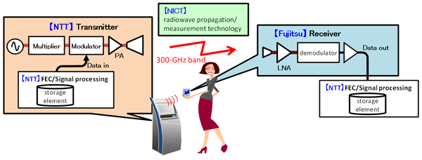
The research is a wide collaboration of Nippon Telegraph and Telephone, Fujitsu and the National Institute of Information and Communications Technology and achieved a transmission rate of 40 gigabits per second through multiplex transmission using orthogonal polarization, enough to transmit a DVD of data in a few seconds. 
As the transceiver can handle a broad frequency band, it is expected to be applied for high-speed wireless communication. An experiment to download a DVD to a compact, smartphone-sized terminal fitted with a matching developed receiver transferred a DVD in 2s.

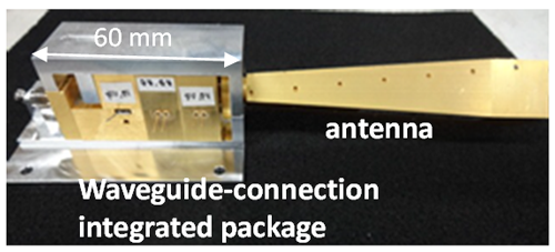
In the experiment, an InP-based high-electron-mobility transistor (InP-HEMT) was used as an ultrahigh-speed device and incorporated in a high-frequency transceiver circuit designed as an integrated circuit (IC). This enabled  20Gbit/s data transmission as an integrated architecture connecting (via a waveguide) a metal package housing the IC and an antenna, and mounting the IC in the antenna-integrated metal package resulted in an overall size of 1 cm3. 

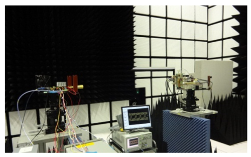
The receiver demodulates a 20Gbit/s wireless signal (received via the wireless section) and outputs it as a data signal. In addition, as for radiowave propagation and measurement technology concerning the 300GHz band, the high-speed data transfer was verified by an experiment performed in an anechoic chamber.

In this verification experiment, the transmitter and a signal processor for forward error correction (FEC) (both developed by NTT), the receiver (developed by Fujitsu), and the radiowave propagation and measurement technology (developed by NICT) were brought together with error free transmission over 1m.


Another experiment on polarization-multiplexing transmission using two transceiver sets and a polarized waves perpendicular to each other showed that 40Gbit/s data transfer is possible. These experiments confirmed sufficient performance as a wireless device transceiver and the utility of the developed technology.

Air transport regulations cause battery headache - updated

By Nick Flaherty www.flaherty.co.uk

New regulations on the shipment of lithium ion batteries by air that came into effect in April are causing headaches for battery makers and customers alike.

The changes came about after several fires on aircraft carrying lithium ion battery packs. Now the charge levels are restricted and the consignments can only be carried in cargo, not passenger planes.

This has also led the US Rechargeable Battery Association (PRBA) to call for tougher enforcement of the transport regulations for battery makers in China. "Unfortunately, we are seeing an enforcement gap in China by agencies overseeing the transport of lithium ion batteries," said George Kerchner, executive director of the PRBA.

The details, with an update on 11/6, are at http://www.power-eetimes.com/news/battery-makers-and-customers-face-transport-challenges, and battery makes such as VARTA Storage are having to add new part numbers to reflect the different levels of charge in the cell. A new design library from VARTA includes all the documentation, certification and 3D models for the batteries to help designers add battery packs quickly and easily.

Thursday, June 09, 2016

Solar cell security system wins Intel and Dell IoT competition

By Nick Flaherty www.flaherty.co.uk

Dell and Intel have unveiled the winners of their “Connect What Matters” IoT Contest.

Over the last six months, businesses large and small have been submitting interesting, practical, data-driven ideas. The overall platinum winner is V5 Systems which has developed a portable, solar-powered security and Industrial IoT system. The technology can be deployed without being tied to power or data cables for applications from law enforcement to agriculture to other outdoor uses. The portable units contain analytics, multiple sensors (including video, acoustic and chemical detection), power, computing and Wi-Fi and cellular communications. 

“As IoT moves from hype to reality, the diversity of applications and use cases among the IoT Innovation contest winners clearly demonstrates the value developers and customers can capture by implementing real IoT solutions,” said Jonathan Ballon, vice president in the Internet of Things Group (IOTG) and general manager of the Markets and Channels Acceleration Division from Intel. “Through our partnership, Dell and Intel are able to provide re-usable building blocks that will help these applications scale in the future.”

Gold winners include:
  • Eigen Innovations who built a video analytics solution that leverages thermal imaging cameras and PLC/sensor data for real-time process and quality control
  • Iamus used its IoT platform and facilities management expertise to build a unique smart streetlamp solution for various applications in smart city project.
  • n.io applied its technology to turn a manually-dependent, subjective farming operation into a highly-instrumented and autonomous example of precision agriculture
  • RiptideIO created a packaged software-as-a-service (SaaS) solution designed to scale in small retail building spaces
  • Software AG built a predictive maintenance solution that includes in memory edge analytics for acting on collected machine data in real-time
Silver winners include AZLOGICA, Blue Pillar, Calibr8 Systems Inc, Daliworks, ELM Energy, Independent Automation, Onstream,PixController, Inc., PV Hardware and We Monitor Concrete.

Dell is expanding its year old IoT Partner Program with VMware, Nokia, Eurotech and others to address new opportunities as the market expands. “We’re proud of the progress that we’ve made this past year,” said Andy Rhodes, executive director, Commercial IoT Solutions, Dell. “With the launch of the Edge Gateway and Embedded Box PCs, our quickly growing partnership program and now our successful IoT Gateway Contest, our efforts underscore Dell’s deep commitment to driving IoT adoption for real world use.”

VMware has qualified its new Liota (Little IoT Agent) open-source software development kit (SDK) with Dell’s IoT hardware, providing customers with further choice for IoT gateway management and the ability to build apps on Dell’s gateway. Liota also acts as a bridge to VMware’s AirWatch and VMware vRealize Operations to allow customers to configure, monitor and deploy millions of things from one console, view device health and act on anomalies as they arise. With Liota open-source SDK, developers can write applications that interact with any data center component, over any transport, for any IoT gateway.

In the spirit of the program, three partners that have demonstrated differentiation have been promoted from the Registered to Associate tier. 
  • DGLogik offers an end-to-end platform for Industrial IoT and Building Automation applications with a particular focus on enabling the rapid creation of rich data visualizations with its DGLux offering. 
  • Exara is collaborating with Dell and Intel to deliver digital oil and gas production optimization solutions that leverage software-based edge data management technology. Exara’s software delivers machine data at any fidelity, any view and always on-demand to enterprise customers and applications without compromising existing industrial control system security or service levels. 
  • FogHorn’s platform is purpose-built to enable edge intelligence and analytics for gateways in Industrial IoT use cases, hosting high performance processing, analytics, and heterogeneous applications closer to control systems and physical sensors. Also joining the program as new Associate partners are KMC Controls, Eurotech, Nokia, and V5 Systems.

“Working together with our customers and partners, including gateway vendors such as Dell, VMware is paving a way for IoT innovation across industries,” said Bask Iyer, chief information officer, VMware. “Our Liota open source SDK provides the libraries to develop apps that connect and orchestrate data and control flows across things, gateways and the cloud.”

www.intel.co.uk/content/www/uk/en/internet-of-things/overview.html

Wednesday, June 08, 2016

WSTS sees dip in chip sales


By Nick Flaherty www.flaherty.co.uk

Is this the start of the cyclical downturn in the semiconductor business? WSTS - the global chip market research group - forecasts that the worldwide semiconductor market will fall 2.4% this year to US$327 billion, but will pick up again in 2017 and 2018.


For 2016, growth in Optoelectronics (1.8%), Sensors (7.6%), and Analogue ICs (1.0%) - mostly driven by industrial, embedded and IoT applications - is expected to be offset by declines in Memory (-10.2%) and Logic (-2.5%). By geography, for 2016, declines are expected across all regions with the largest decline in Americas.
For 2017 and 2018, all major product categories and all regions are forecasted to grow reaching US$341 billion in 2018. As a result, the worldwide semiconductor market is forecasted to be up ~2% year-on-year in both 2017 and 2018, which is not the large growth that gives confidence and any small downturn can turn this to a drop.

By region, a positive growth rate is projected for all regions in 2017 and 2018. The Americas and Asia Pacific regions are expected to show the highest growth rate, accounting for approximately 80% of the market.

What are the most influential products to use MIPS or PowerVR?

By Nick Flaherty www.flaherty.co.uk

Last month TIME magazine tried to compile the ultimate tech catalogue counting down 50 of the most influential gadgets of all time. They put the Raspberry Pi at 45, close to the Segway at 48, but this got the engineers at Imagination Technologies  thinking about the most iconic products to use MIPS CPUs and PowerVR GPUs

(By the way, the top product for TIME was the iPhone)

After careful deliberation, here are the top picks from Imagination, from the PowerVR graphics in the original iPhone to the MIPS-based Nintendo N64 and the SGI Indigo workstation:
 

#TeamPowerVR

  1. The Matrox m3D graphics card
  2. The SEGA Dreamcast game console
  3. The Samsung Galaxy S smartphone
  4. The Sony PlayStation Vita portable game console
  5. The original Apple iPhone

#TeamMIPS

  1. The SGI Indigo workstation
  2. The original Sony PlayStation game console
  3. The Nintendo N64 game console
  4. The NEC Cenju-4 supercomputer
  5. The Tesla Model S electric car
To pick your favorite from the two lists, simply click on the links below and vote in our poll!

http://blog.imgtec.com/powervr/five-most-influential-devices-to-use-powervr-gpus

http://blog.imgtec.com/mips-processors/five-most-iconic-devices-to-use-mips-cpus 
 

Tuesday, June 07, 2016

Cadence and Mentor square off in design of custom IoT chips

By Nick Flaherty www.flaherty.co.uk


The growth of the Internet of Things and the large volumes for chips is creating new interest in developing custom chips for embedded applications, and two of the largest tool providers are going head to head with a low cost design flow.

While ARM is offering its M0 processor core free to evaluate (and a lower cost $40,000 commercial license), the challenge is developing a mixed signal analogue and digital chip. While Cadence Design Systems has traditionally dominated the analogue portion of the chip design flow, Mentor Graphics recently bought the analogue and MEMS design tools of Tanner, providing a competing flow.   

The custom chips can be produced at relatively low cost as part of a 180nm multi-project wafer from a supplier such as Europractice which can provide 45 samples of a 25mm2 chip for $16,000. With a relatively small production run of 100,000 chips, this NRE engineering cost becomes quite affordable.

The Cadence offering accelerates mixed-signal SoC design for IoT, incorporating the ARM IoT Subsystem for Cortex-M processors and Cadence’s interface IP and unified mixed-signal implementation solution, now optimized specifically for Cortex-M cores. The design flow integrates the Virtuoso custom design platform with the Innovus Implementation System, and the Spectre custom verification platform with the Incisive Enterprise Simulator provides the basis for ARM-based IoT design and verification.

These tools are not cheap, so further lower the barriers to the chip development, Cadence has also joined the ARM DesignStart program to provide low cost tools and IP for designs incorporating the Cortex-M0 processor. This offers potential chip designers access to free Cortex-M0 processor IP for design, simulation, and prototyping, with the option of then purchasing a simplified fast-track license for commercialization.

The ARM IoT Subsystem and DesignStart packages provide the most comprehensive solution a designer may need – including tools and IP – to accelerate time-to-silicon for their IoT applications.  The combined mixed-signal IoT flow for both the IoT subsystem package and DesignStart are available on the Cadence Hosted Design Solution (HDS), a software-as-a-service (SaaS) model which offers quick access to EDA tools, support and methodologies. With this secure solution, users can log in anywhere, anytime and gain access to tools without needing installation or the supporting hardware for it.

Optimizing IoT system design requires a deep understanding of tool flows, methodology, IP, packaging and software. ARM has developed a test chip to showcase this complete IoT implementation using a complete Cadence tool flow, the ARM IoT Subsystem and Cadence IP. The test chip includes processor IP, Artisan physical IP, wireless connectivity solutions, interface IP, software, design tools (both front- and back-end), optimized design methodology and scripts.

“ARM is seeing a growing demand for custom SoCs as our partners continue to focus on improving costs, power and functionality,” said Vincent Korstanje, vice president of marketing, systems & software group at ARM. “The collaboration with Cadence makes designing IoT platforms and custom SoCs even easier, further accelerating time to market.”

“We are collaborating with ARM to provide a complete solution of optimized IP, tool flows and subsystems to enable customers to deliver emerging Internet of Things applications,” said Dr. Chi-Ping Hsu, senior vice president and chief strategy officer, Cadence. “Through our continued collaboration with ARM on both ARM DesignStart and the ARM IoT Subsystem for Cortex-M, we’ve optimized our EDA tools and methodology to complement ARM IP to bring designers from concept to silicon much faster.”

But Mentor is also joining the party through a similar collaboration using the Tanner AMS analogue/mixed-signal design flow for M0 processor-based implementations as part of the DesignStart program. The collaboration lowers the barriers to embedded and IoT device design and verification through a combination of an affordable, complete IC design tool suite and the ability to evaluate the design flow on a reference design at no cost.

“The free evaluation environment and an affordable tool suite from Tanner gives any vendor a fast and effective way to develop Cortex-M0 based smart analog mixed-signal designs,” said Nandan Nayampally, vice president of marketing and strategy, CPU Group at ARM. “Our partnership with Mentor Graphics will streamline the path to full production of IoT and embedded products, reducing developers’ costs and increasing their speed to market.”

The Tanner design flow supports digital, analogue, AMS, and MEMS design in a highly integrated, end-to-end flow. Designers capture the schematic, perform analogue and mixed-signal simulation, and lay out and verify the physical design. This design flow offers a complete, processor-based IoT chip environment.

Designers will be able to evaluate an ARM Cortex-M0 IoT reference design at no cost by using a web-based Mentor Virtual Lab to interact with the complete set of Tanner design tools. After evaluation, customers can easily purchase the specially-priced software from Tanner to begin creating their own IoT designs and combine this with the free Cortex-M0 design access available on the ARM DesignStart portal.

“The Tanner design flow is already very popular with IoT design companies,” said Greg Lebsack, general manager of the Tanner EDA business unit at Mentor Graphics. “By collaborating with ARM on DesignStart, we further strengthen our design flow by making it easy for AMS designers to include an ARM Cortex-M0 processor in their IoT designs.”

ARM of course wants to have more and more chip suppliers in the IoT. The new ARM Approved Design Partner program also provides DesignStart users with a global list of audited design houses for expert support during development.

The DesignStart portal offers SoC designers free access to ARM Cortex-M0 processor IP for design, simulation and prototyping with the option to buy a simplified and standardized $40,000 fast track license. The addition of Cadence and Mentor Graphics tools for DesignStart users accelerates the development of custom SoCs for embedded and Internet of Things (IoT) applications. With test chips from as little as $16,000 to manufacture (not inclusive of EDA tooling and IP licensing costs), the path to custom SoCs is now much easier.

ARM’s DesignStart portal, with its convenient access to the Cortex-M0 package and its low-cost path to commercialization, is already making it easier for start-ups and OEMs to create embedded and mixed-signal SoCs,” said Nandan Nayampally, vice president of marketing and strategy for the CPU group at ARM. “Simplifying access to EDA tools from Cadence and Mentor Graphics will further spur rapid innovation, creating a fast path to production silicon for companies looking to deliver an embedded or connected IoT product.”


The Approved Design Partner program helps designers with the chip implementation. “The semiconductor industry has high expectations for future growth in the IoT space, with DesignStart ARM has taken a significant step towards enabling this growth and lowering entry barriers,” said Graham Curren, CEO at one design partner, Sondrel. 

IoT drives Ethernet switching into embedded

By Nick Flaherty www.flaherty.co.uk

Switch Silicon and Software Optimized for Industrial Ethernet Applications Targets Industrial Internet of Things Market


Microsemi has launched a new family of low power Ethernet switches for the growing Industrial Internet of Things (IIoT) market.

Designed for the specific needs of industrial applications such as factory automation, process control, smart grid/smart energy and physical security, the Ocelot switches simplify IIoT network migration to an Ethernet backbone with flexible interfaces, TCAM based classifications, 1588 timing and ring protection in a small package.

“Ethernet’s use in industrial communications is increasingly widespread as the industry looks to modernize their networks onto this ubiquitous standard,” said Larry O’Connell, director of product marketing at Microsemi. “The addition of our new Ocelot devices expands our portfolio and provides IIoT customers with a cost-effective solution that does not compromise on features.”

According to ARC Advisory Group, the industrial Ethernet switch market is now over $1 billion annually and expected to grow at double-digit rates for the next five years.

Microsemi’s Ocelot family includes:
• VSC7511, a four-port, layer 2 gigabit Ethernet switch with four fully integrated copper PHYs (shown above)
• VSC7512, a 10-port, layer 2 gigabit Ethernet switch with four fully integrated copper PHYs
• VSC7513, an eight-port, layer 2/3 gigabit Ethernet switch
• VCS7514, a 10-port layer 2/3 gigabit Ethernet switch

In addition to using Microsemi’s technology to offer low power, small package sizes, 1588 timing and ring protection, the Ocelot switches feature optimised port configurations, unmanaged and managed options, and IStaX software optimized for the industrial market.

The family is sampling now, with production scheduled for summer 2016. Evaluation boards for the devices are available now.

Quadium raises $20m for IoT device analytics software

By Nick Flaherty www.flaherty.co.uk

US startup Quadium has raised $20m to manage, monitor and protect devices in the Internet of Things as the battle for IoT analytics heats up.

Starting from a defence and military background, Qadium built a platform to index every device on the public internet and to identify relationships between those devices at scale for corporate and government cybersecurity applications. Results are made available to customers in a software product called Expander. However, this comes with associated 'professional services' aka consulting, which may demonstrate that we have a long way to go to automate this processes. 

The Quadium platform sends signals across the public internet space, interpreting returned data to determine what devices are running where, and building network graphs to understand relationships between those devices. This empowers workflows associated with mapping one’s presence on the global internet, even for networks with millions of IPs and many active devices. Qadium routinely sees hundreds of millions of devices on the public internet when it conducts its sensing, and has seen many billions since it started gathering its data.

This internet-scale perspective allows customers to “observe their networks as an adversary would over the global internet, and they are often surprised by what they see” according to retired Admiral James Winnefeld, former Vice Chairman of the Joint Chiefs of Staff, who is an advisor to the company.

Customers in the private sector include Fortune 500 companies in financial services, insurance, healthcare, defence industry, auditing and consulting, and retail. Enterprise networks are no longer enclaves to guard; interdependencies with cloud service providers, credentialed vendors, employees’ devices, and more create porous perimeters that can only be defended with a whole-of-internet approach. David Dorman, technology investor and former CEO of AT&T, affirms that “Qadium’s Expander software is the only enterprise product that monitors the entire device layer of the internet for customer weaknesses.”

Qadium’s co-founders met while working as consultants at DARPA, the Pentagon’s research agency, and won over $10 million in multi-year DoD contracts to begin development of its internet sensing and data analysis prototypes. Qadium has since begun operational transitions to military services, including US Cyber Command. “All of Qadium’s government work is defensive in nature,” said Junio. “We have very strict protocols in place to ensure that we never participate in offensive cyber warfare by any government, including the US.”

The team is largely recruited out of algorithms research groups at Stanford, Caltech, and MIT, and software engineers with top-of-industry experience.

“The secret to how Qadium solved technology problems that no one else could,” says Shaun Maguire, co-founder and chairman, “it is in its people. Only an interdisciplinary group of top minds could have built an end-to-end system of this scope and complexity while delivering profound new insights to the world’s most demanding customers.”

Qadium previously raised $6 million in a seed round that closed in summer 2015. The seed round was led by Founders Fund (Peter Thiel), joined by OATV (Mark Jacobsen), Susa Ventures (Seth Berman), and a group of angel investors. The company intends to spend the money on scaling its core business, including improving its global sensing to continually increase the rate at which customers receive alerts to relevant changes.

Friday, June 03, 2016

TI extends its lead in the top ten analogue semiconductor companies

By Nick Flaherty www.flaherty.co.uk


The 2015 analogue market grew 2% to $47.0 billion, a positive sign set against the recent fall sin the overall, memory-led market. Even though it has a dominant 18% market share, Texas Instruments grew faster than the market at 3% and is by far the dominant supplier.

Combined sales of general-purpose analogue products such as amplifiers/comparators, interface, power management and signal conversion devices increased 2% to $19.1 billion and sales of application-specific analogue devices also improved 2% to $27.9 billion. The market for signal conversion devices showed the largest increase in 2015, growing 14% to $2.9 billion.

IC Insights’ ranking of the top analogue IC suppliers for 2015 show the top ten accounted for 56% of global analogue sales last year, down slightly from 57% in 2014. Among the top suppliers, only tenth-ranked Renesas fell short of the $1.0 billion mark. With a 10% increase, NXP’s analogue sales outperformed the total analogue market by the widest margin, while ST saw the biggest drop at 13%..


TI’s analogue sales slightly surpassed the combined revenue of the next three-largest analog suppliers, and represented 69% of its total semiconductor revenue last year. TI has always been a major player in analogue, but beginning in 2009, it doubled down on its long-term efforts to dominate this market segment says IC Insights. That year, TI became the first company to manufacture analog devices on 300mm equipment. It purchased 300mm manufacturing tools from defunct Qimonda and transferred it to its existing fabs in Texas to build analogue chips. In 2010, TI acquired two wafer fabs operated by Spansion in Aizu-Wakamatsu, Japan, and a fully equipped 200mm fab in Chengdu, China from Cension Semiconductor Manufacturing. Both facilities were converted and immediately put to use making analog ICs. In April 2011, TI acquired National Semiconductor—its rival in many analogue markets—for $6.5 billion.

TI also strengthened its analogue position by transitioning to 300mm manufacturing capacity at its newer RFAB and its older DMOS 6 fabs. Aside from boosting its manufacturing capacity, moving to 300mm wafer helped reduce total production costs by 40%, according to the company.

Other changes seen in the 2015 ranking include Infineon moving up one place to become the second-largest analogue supplier and Skyworks Solutions moving up two spots. ST slipped from #2 in 2014 to #5 in the 2015 ranking following its 13% decline in analogue sales, which it attributed to soft equipment sales (computer, consumer, automotive, industrial) among its primary customers. Collectively, Infineon, NXP, and ST—Europe’s three-largest IC suppliers—accounted for 15% analogue marketshare last year.

Skyworks continues to enjoy solid analogue sales due to design wins with smartphones providers around the world. Skyworks Solutions makes analogue and mixed signal semiconductors for Apple, Samsung, and other suppliers of mobile devices. Many of Skyworks’ power amplifier components are found in Apple’s iPhone 6 models. It has been estimated that Skyworks supplies $4 worth of content for every iPhone 6 handset.

Although highly focused in mobile markets, Skyworks plans to expand into the automotive, home, and wearable markets to develop its presence in applications linked to the Internet of Things. Analogue chips such as audio amplifiers, op amps, and analog switches are building blocks for creating wearable applications. Skyworks’ wireless technology is used in General Electric healthcare equipment, and the company recently sealed a deal to supply high-performance filter solutions to Panasonic.

Analog Devices’ analogue sales grew 2% last year with one of its key devices enabling the 3D/Force Touch capability in the Apple Watch, the latest iPhones, and new generations of the iPad. This uses tiny electrodes to distinguish between a light tap and a deep press to trigger contextually specific controls.

Things are also looking up for the market, as IC Insights forecasts the total analogue market to grow 4% this year, reaching $49.1 billion and surpassing the $50.0 billion mark for the first time in 2017 as analogue sales climb to an expected $51.4 billion. From 2015 to 2020, the analogue market is forecast to grow at a compound annual growth rate of 6%, one point higher than the total IC market.

Downturn hits top 20 semiconductor companies in 2016

By Nick Flaherty www.flaherty.co.uk

The latest report from US market researchers IC Insights is showing the impact of the cyclical downturn in the semiconductor industry on the top 20 suppliers. Of these top 20 companies, it is mergers that are providing the growth in the first quarter, such as Intel's acquisition of Altera, although both the Broadcom/Avago combination and NXP/Freescale saw declines.


All three main foundries -TSMC, UMC and Global Foundries, saw a year on year decline, highlighting the general challenge of the market, along with the drop in memory prices hitting companies such as Samsung. Intel, NVIDIA, Infineon and Mediatek were the only companies to see growth.

www.ICinsights.com


Thursday, June 02, 2016

'On-the-fly' 3-D print system prints what you design, as you design it - video

By Nick Flaherty www.flaherty.co.uk

Researchers at Cornell University in the US have developed an interactive prototyping system that prints what you are designing as you design it; the designer can pause anywhere in the process to test, measure and, if necessary, make changes that will be added to the physical model still in the printer.

"We are going from human-computer interaction to human-machine interaction," said graduate student Huaishu Peng. Their system uses an improved version of an innovative "WirePrint" printer developed in a collaboration between Guimbretière's lab and the Hasso Platner Institute in Potsdam, Germany.


THIS WIRE FRAME PROTOTYPE OF A TOY AIRCRAFT WAS PRINTED IN JUST 10 MINUTES, INCLUDING TESTING FOR CORRECT FIT, AND MODIFIED DURING PRINTING TO CREATE THE COCKPIT.  CREDIT: CORNELL UNIVERSITY

In conventional 3-D printing, a nozzle scans across a stage depositing drops of plastic, rising slightly after each pass to build an object in a series of layers. With the WirePrint technique the nozzle extrudes a rope of quick-hardening plastic to create a wire frame that represents the surface of the solid object described in a computer-aided design (CAD) file. WirePrint aimed to speed prototyping by creating a model of the shape of an object instead of printing the entire solid. The On-the-Fly-Print system builds on that idea by allowing the designer to make refinements while printing is in progress.

The new version of the printer has "five degrees of freedom." The nozzle can only work vertically, but the printer's stage can be rotated to present any face of the model facing up; so an airplane fuselage, for example, can be turned on its side to add a wing. There is also a cutter to remove parts of the model, say to give the airplane a cockpit.

The nozzle has been extended so it can reach through the wire mesh to make changes inside. A removable base aligned by magnets allows the operator to take the model out of the printer to measure or test to see if it fits where it's supposed to go, then replace it in the precise original location to resume printing.

The software - a plug-in to a popular CAD program - designs the wire frame and sends instructions to the printer, allowing for interruptions. The designer can concentrate on the digital model and let the software control the printer. Printing can continue while the designer works on the CAD file, but will resume when that work is done, incorporating the changes into the print.

As a demonstration the researchers created a model for a toy airplane to fit into a Lego airport set. This required adding wings, cutting out a cockpit for a Lego pilot and frequently removing the model to see if the wingspan is right to fit on the runway. The entire project was completed in just 10 minutes.

By creating a "low-fidelity sketch" of what the finished product will look like and allowing the designer to redraw it as it develops, the researchers said, "We believe that this approach has the potential to improve the overall quality of the design process."