$2.3bn deal to build smart grid leader
By Nick Flaherty www.flaherty.co.uk
Toshiba is to buy Landis+Gyr for $2.3bn to build the world leader in Smart Grid technology.
The acquisition is designed to create a new platform within Toshiba specifically targeting the global Smart Grid opportunity for both utility customers and consumers. Landis+Gyr has over 8,000 utility customers around teh world and has been pioneering smart metering, networking and service products.
“We welcome Landis+Gyr, the world leader in smart metering products and services, to the Toshiba family” said Hideo Kitamura, Toshiba’s Corporate Executive Vice President . “Our intent is to become a global leader in the Smart Community business by 2020. Together with Landis+Gyr, we will accelerate the development of our combined product and service portfolio to empower utilities and their end customers and to provide sophisticated Smart Community solutions in the global market.”
Toshiba says it will retain and enhance the globally respected Landis+Gyr brand, and continue to meet and exceed customer requirements worldwide. There are no plans for job reduction or restructuring as a result of this transaction.
“Over the past 10 years we have built the world leader in smart metering,” said Landis+Gyr CEO Andreas Umbach. “As a growth platform for Toshiba, Landis+Gyr will have the resources and power to complement, and indeed accelerate, our product offering to utilities. With this transaction, Toshiba will now share our vision of helping the world manage energy better”.
‘The shareholders and I are very proud to have come this far in creating a global leader in an essential industry undergoing transformational growth,” said Cameron O’Reilly, the founder of the investment group that has supported the building of Landis+Gyr over the past 9 years. “We are delighted that Toshiba fully shares our vision, and intends to take Landis+Gyr to the next stage in its exciting development”. Major shareholders of the selling Landis+Gyr investor group include interests associated with Allianz Capital Partners, Australian Capital Equity, DLJ Merchant Banking Partners, Dubai International Capital, Marinya Holdings, Sir Douglas Myers, Sir Anthony O’Reilly, Propel Investments, and Sofina.
All the latest quantum computer articles
See the latest stories on quantum computing from eeNews Europe
Thursday, May 19, 2011
Wednesday, May 18, 2011
SanDisk buys Pliant for SSD market
By Nick Flaherty www.flaherty.co.uk
Flash chip maker SanDisk has bought solid state disk company Plaint Technology in a $327m deal to catapult the company into the SSD market.
Pliant, whos new CEO started last month, currently sells ultra-high performance enterprise solid state drives based on multi-level cell flash memory and the SAS protocol to meet the performance, data integrity and reliability needs of enterprise storage customers. The company's product roadmap also includes PCIe-based solutions for high-performance compute servers.
"Flash memory is making significant inroads into the enterprise by dramatically increasing application performance and reducing power consumption," said Sanjay Mehrotra, SanDisk president and chief executive officer. "We believe that the combination of Pliant's innovative technology and enterprise-level system expertise with SanDisk's high-quality, large-scale MLC memory production is a winning value proposition for customers. Our advanced flash technology roadmap and flash management capability will complement Pliant's strengths and allow us to lead the way in reliability and performance in the Enterprise SSD market."
"Pliant has had initial success in the enterprise SAS SSD market, which is that company's sole focus," said Jim Handy at Objective Analysis. "The enterprise SSD market is the fastest-growing SSD market and is one that SanDisk has not targeted so far - SanDisk has dedicated the majority of its SSD efforts to the client PC SSD market, a market that has not materialized to the extent expected by its advocates for the past several years. Most PC buyers still don't want an SSD enough to pay the high price for the amount of storage they get."
"Through this acquisition SanDisk can suddenly jump into the enterprise SSD market at full speed with a device that is already production qualified and with established relationships and design wins with key customers in that market," he said.
Flash chip maker SanDisk has bought solid state disk company Plaint Technology in a $327m deal to catapult the company into the SSD market.
Pliant, whos new CEO started last month, currently sells ultra-high performance enterprise solid state drives based on multi-level cell flash memory and the SAS protocol to meet the performance, data integrity and reliability needs of enterprise storage customers. The company's product roadmap also includes PCIe-based solutions for high-performance compute servers.
"Flash memory is making significant inroads into the enterprise by dramatically increasing application performance and reducing power consumption," said Sanjay Mehrotra, SanDisk president and chief executive officer. "We believe that the combination of Pliant's innovative technology and enterprise-level system expertise with SanDisk's high-quality, large-scale MLC memory production is a winning value proposition for customers. Our advanced flash technology roadmap and flash management capability will complement Pliant's strengths and allow us to lead the way in reliability and performance in the Enterprise SSD market."
"Pliant has had initial success in the enterprise SAS SSD market, which is that company's sole focus," said Jim Handy at Objective Analysis. "The enterprise SSD market is the fastest-growing SSD market and is one that SanDisk has not targeted so far - SanDisk has dedicated the majority of its SSD efforts to the client PC SSD market, a market that has not materialized to the extent expected by its advocates for the past several years. Most PC buyers still don't want an SSD enough to pay the high price for the amount of storage they get."
"Through this acquisition SanDisk can suddenly jump into the enterprise SSD market at full speed with a device that is already production qualified and with established relationships and design wins with key customers in that market," he said.
"The Enterprise SSD market is poised for considerable growth, with revenue projected to reach $4.2 billion in 2015, up from $994 million in 2010," according to Joseph Unsworth, research director at Gartner. "This trajectory is fueled by the expanding use of MLC NAND technology, which will require extensive flash management expertise to ensure successful adoption in enterprise applications."
"Something striking about this deal is the absence of overlap between the two companies," said Handy. "In design, SanDisk has great strengths in NAND flash and NAND controllers, SATA, USB, and flash card interfaces. Pliant has some flash controller expertise, but also brings significant strengths that SanDisk lacks in SAS interface technology, high-speed SSD data management, and end-to-end data protection."
"SanDisk's sales & marketing strengths include retail sales and OEM sales to cell phone and tablet PC makers," he added. "Pliant's sales and marketing efforts are narrowly focused on enterprise server makers and storage array OEMs. In short, there seems to be a near-ideal lack of redundancies that is rare in companies that bring synergies to the market."
"Something striking about this deal is the absence of overlap between the two companies," said Handy. "In design, SanDisk has great strengths in NAND flash and NAND controllers, SATA, USB, and flash card interfaces. Pliant has some flash controller expertise, but also brings significant strengths that SanDisk lacks in SAS interface technology, high-speed SSD data management, and end-to-end data protection."
"SanDisk's sales & marketing strengths include retail sales and OEM sales to cell phone and tablet PC makers," he added. "Pliant's sales and marketing efforts are narrowly focused on enterprise server makers and storage array OEMs. In short, there seems to be a near-ideal lack of redundancies that is rare in companies that bring synergies to the market."
Related articles
- SanDisk to buy SSD maker Pliant for $327 million (macworld.com)
- Pliant puts shiny new CEO to work (go.theregister.com)
- SanDisk buying SSD developer Pliant Technology (news.cnet.com)
- SanDisk Acquires Flash Disk Maker Pliant Technology For $327M Plus Earn-out (techcrunchit.com)
- SanDisk gobbles Pliant in $327m deal (go.theregister.com)
- SanDisk outs 19nm flash memory monolithic chip (slashgear.com)
- SanDisk and Toshiba One-Up Intel, Intro 19nm Flash Memory (pcworld.com)
- Samsung producing DDR 2.0 NAND flash (macworld.com)
AMC launches compact Atom embedded PC
Only 1U in height and 120mm square
By Nick Flaherty www.flaherty.co.uk
Advanced Modular Computers has introduced two new highly-compact industrial computers targeted at industrial thin-client applications or distributed processing nodes such as those found in production lines. The small form factor and rugged construction is ideal for mounting within existing equipment or in inaccessible locations. This is aided by a very flexible set of fixing options, such as VESA 75, VESA 100 and wall-mount. as well as wireless, 4 x USB ports, 2 x serial ports and GB Ethernet.
A Compact Flash socket and two SD slots for storage extension provides all the memory capacity needed for an embedded application.
Key Features:
• Atom CPU at 1.1GHz
• Dual Internal SD card slot
• 1GB On-board memory
• MPEG2, WMV9/VC1 Graphics
• 5 Volt Only Power required
• VESA 75 Mountable
• Integrated Audio
• Gigabit Ethernet
• Wireless option
• Rugged metal construction
• Only 10W power consumption
Contact AMC for details

By Nick Flaherty www.flaherty.co.uk
Advanced Modular Computers has introduced two new highly-compact industrial computers targeted at industrial thin-client applications or distributed processing nodes such as those found in production lines. The small form factor and rugged construction is ideal for mounting within existing equipment or in inaccessible locations. This is aided by a very flexible set of fixing options, such as VESA 75, VESA 100 and wall-mount. as well as wireless, 4 x USB ports, 2 x serial ports and GB Ethernet.
A Compact Flash socket and two SD slots for storage extension provides all the memory capacity needed for an embedded application.
Key Features:
• Atom CPU at 1.1GHz
• Dual Internal SD card slot
• 1GB On-board memory
• MPEG2, WMV9/VC1 Graphics
• 5 Volt Only Power required
• VESA 75 Mountable
• Integrated Audio
• Gigabit Ethernet
• Wireless option
• Rugged metal construction
• Only 10W power consumption
Contact AMC for details

Related articles
- Fanless industrial PCs have CompactFlash, Mini PCI Express expansion (linuxfordevices.com)
Tuesday, May 17, 2011
New MRAM plant for Russia
Joint venture with Crocus of the US
By Nick Flaherty www.flaherty.co.uk
Crocus Technology, a US developer of MRAM technology is teaming up with the RUSNANO Russian nano-technology investment fund to start a new manufacturing joint venture with a combined investment totaling $300 million. Under the agreement, Crocus and RUSNANO will form Crocus Nano Electronics (CNE), to build an advanced MRAM facility in Russia, capable of manufacturing medium to high density MRAM products based on Crocus' Thermally Assisted Switching (TAS) MRAM technology at 90nm and 65nm lithographies.
Approximately $125 million will be invested in the first year for setting up CNE's MRAM facility in Russia. In addition, RUSNANO along with Crocus' existing investors CDC Innovation, Ventech, IDInvest Partners, NanoDimension, and Sofinnova Ventures will make an equity investment of $55 million into Crocus. An additional $120 million is slated to be deployed in subsequent years to increase production capability of the MRAM facility. Further investment to support upgrades to 45nm and finer lithographic processing is also incorporated into this agreement.
By Nick Flaherty www.flaherty.co.uk
Crocus Technology, a US developer of MRAM technology is teaming up with the RUSNANO Russian nano-technology investment fund to start a new manufacturing joint venture with a combined investment totaling $300 million. Under the agreement, Crocus and RUSNANO will form Crocus Nano Electronics (CNE), to build an advanced MRAM facility in Russia, capable of manufacturing medium to high density MRAM products based on Crocus' Thermally Assisted Switching (TAS) MRAM technology at 90nm and 65nm lithographies.
Approximately $125 million will be invested in the first year for setting up CNE's MRAM facility in Russia. In addition, RUSNANO along with Crocus' existing investors CDC Innovation, Ventech, IDInvest Partners, NanoDimension, and Sofinnova Ventures will make an equity investment of $55 million into Crocus. An additional $120 million is slated to be deployed in subsequent years to increase production capability of the MRAM facility. Further investment to support upgrades to 45nm and finer lithographic processing is also incorporated into this agreement.
However, this is nowhere near enough cash for a 65nm plant, let alone a 45nm operation. While there may be facilities available for such a plant, the equipment cost is going to limit the production volume at this investment level.
The Russia-based CNE facility will use Crocus' technology to create the first dedicated magnetic memory wafer fab in the world capable of high volume manufacturing of MRAM devices on 300mm wafers with 90nm and 65nm feature sizes. The factory will be designed to add MRAM specific processing layers to standard CMOS foundry wafers. The production facility is scheduled to be in operation within two years and will be capable of producing up to 500 wafers per week.
Expanded capacity of up to 1000 wafers per week is anticipated under a second phase of investment. In addition, CNE and Crocus plan to create a Learning Centre and a Development Ecosystem for advanced memory design and production in the Russian Federation. Crocus will invest over $5 million initially into Russian research organizations to develop advanced manufacturing solutions. This research investment will expand over time to include system-on-chip (SOC) capabilities for secure memory, network processing, and advanced computing.
"RUSNANO's investment reflects their commitment to breaking down international divides to stimulate the global nano-technology industry," said Bertrand F. Cambou, executive chairman of Crocus Technology. "We are pleased that RUSNANO has chosen to invest in Crocus' technology and is actively participating in building a unique Russian-based manufacturing facility that will serve a global market."
"We selected Crocus because we believe their technology is best-in-class and promises to bring differentiated MRAM products to market", said Anatoly Chubais, CEO and chairman of the Executive Board of RUSNANO, which started life in March and is 100% owned by the Russian Federation. It has already made $5.9bn of investments. "Crocus' executive team has a rich history of cooperation with Russian researchers. CNE and Crocus will be important elements of RUSNANO's strategy for establishing the microelectronics industry in Russia based on the world's best technology."
CNE's 90nm & 65nm manufacturing capability will enable Crocus to offer much higher density MRAM devices than currently available. Products manufactured by CNE will be marketed and sold worldwide by Crocus, excluding Russia and other former CIS states, while CNE will market directly within the former CIS. Crocus products sourced by CNE will address key markets such as storage, mobile communications, networking and cloud computing. In addition to general purpose memory applications, Crocus' TAS MRAM technology will serve specific uses in smartcards, network processing, biometric authentication, near-field communications (NFC), and secure memory. The unlimited endurance, non-volatility, and fast read/write performance of Crocus' MRAM technology are extremely valuable for many of these applications. Crocus' technology will be available for use in both standalone and embedded applications, addressing a total market opportunity of more than$40 billion per year.
The CNE joint venture will be complementary to Crocus' previously announced wafer foundry partnership with TowerJazz, which has successfully entered the final qualification stage, with production ramp of 130nm MRAM devices planned for late 2011. In addition, Crocus will continue to work with SVTC, its process integration R&D partner in San Jose, CA, to develop key manufacturing process steps to be used by CNE
CNE's 90nm & 65nm manufacturing capability will enable Crocus to offer much higher density MRAM devices than currently available. Products manufactured by CNE will be marketed and sold worldwide by Crocus, excluding Russia and other former CIS states, while CNE will market directly within the former CIS. Crocus products sourced by CNE will address key markets such as storage, mobile communications, networking and cloud computing. In addition to general purpose memory applications, Crocus' TAS MRAM technology will serve specific uses in smartcards, network processing, biometric authentication, near-field communications (NFC), and secure memory. The unlimited endurance, non-volatility, and fast read/write performance of Crocus' MRAM technology are extremely valuable for many of these applications. Crocus' technology will be available for use in both standalone and embedded applications, addressing a total market opportunity of more than$40 billion per year.
The CNE joint venture will be complementary to Crocus' previously announced wafer foundry partnership with TowerJazz, which has successfully entered the final qualification stage, with production ramp of 130nm MRAM devices planned for late 2011. In addition, Crocus will continue to work with SVTC, its process integration R&D partner in San Jose, CA, to develop key manufacturing process steps to be used by CNE
Related articles
- Russia to Invest in U.S. Memory Chip Firm [Voices] (voices.allthingsd.com)
- Extremely fast MRAM data storage within reach (physorg.com)
- MRAM data storage with 500 picosecond response (nextbigfuture.com)
- Rusnano chief urges investment in Russia's nanotech startups (en.rian.ru)
- Nanostart launches nanotechnology fund in Russia (finanznachrichten.de)
Silicon Image sets up new 60GHz wireless division after SiBeam acquisition
By Nick Flaherty www.flaherty.co.uk
Multimedia chip designer Silicon Image is setting up a wireless division following the $25m acquisition of 60GHz chip pioneer SiBeam.
“The SiBEAM acquisition supports our long-term growth strategy to offer a full range of HD connectivity options based on wired and wireless industry standards,” said Camillo Martino, chief executive officer of Silicon Image, Inc. “SiBEAM’s 60GHz Radio Frequency (RF) technology complements our HD connectivity portfolio by adding WirelessHD-compliant semiconductor products that deliver the highest throughput of any mass market wireless solution available today.”
As a result of the acquisition, Silicon Image’s headcount will increase by approximately 50 people to a total worldwide headcount of approximately 500 employees. SiBEAM’s high-speed wireless communication products will be integrated into Silicon Image’s newly formed Wireless Division, headed by John LeMoncheck, former president and chief executive officer of SiBEAM and Silicon Image’s new vice president and general manager, Wireless Division, reporting to Martino.
“We are excited to be part of the Silicon Image team and are looking forward to delivering a world class wireless product portfolio that combines the strengths of SiBEAM’s 60GHz technology with Silicon Image’s leadership in HD connectivity products,” said LeMoncheck.
Multimedia chip designer Silicon Image is setting up a wireless division following the $25m acquisition of 60GHz chip pioneer SiBeam.
“The SiBEAM acquisition supports our long-term growth strategy to offer a full range of HD connectivity options based on wired and wireless industry standards,” said Camillo Martino, chief executive officer of Silicon Image, Inc. “SiBEAM’s 60GHz Radio Frequency (RF) technology complements our HD connectivity portfolio by adding WirelessHD-compliant semiconductor products that deliver the highest throughput of any mass market wireless solution available today.”
As a result of the acquisition, Silicon Image’s headcount will increase by approximately 50 people to a total worldwide headcount of approximately 500 employees. SiBEAM’s high-speed wireless communication products will be integrated into Silicon Image’s newly formed Wireless Division, headed by John LeMoncheck, former president and chief executive officer of SiBEAM and Silicon Image’s new vice president and general manager, Wireless Division, reporting to Martino.
“We are excited to be part of the Silicon Image team and are looking forward to delivering a world class wireless product portfolio that combines the strengths of SiBEAM’s 60GHz technology with Silicon Image’s leadership in HD connectivity products,” said LeMoncheck.
New solar product claims capture of up to 95 percent of light energy
Consumer production in five years
By Nick Flaherty www.flaherty.co.uk

A University of Missouri engineer has developed a flexible solar sheet that captures more than 90 percent of available light, and he plans to make prototypes available to consumers within the next five years.
Patrick Pinhero, an associate professor in the MU Chemical Engineering Department, says energy generated using traditional photovoltaic (PV) methods of solar collection is inefficient at around 20% and neglects much of the available solar electromagnetic (sunlight) spectrum.
By Nick Flaherty www.flaherty.co.uk
A University of Missouri engineer has developed a flexible solar sheet that captures more than 90 percent of available light, and he plans to make prototypes available to consumers within the next five years.
Patrick Pinhero, an associate professor in the MU Chemical Engineering Department, says energy generated using traditional photovoltaic (PV) methods of solar collection is inefficient at around 20% and neglects much of the available solar electromagnetic (sunlight) spectrum.
The device his team has developed is essentially a thin, moldable sheet of small antennas called nantenna that can harvest the heat from industrial processes and convert it into usable electricity. Their ambition is to extend this concept to a direct solar facing nantenna device capable of collecting solar irradiation in the near infrared and optical regions of the solar spectrum.
Working with his former team at the Idaho National Laboratory and Garrett Moddel, an electrical engineering professor at the University of Colorado, Pinhero and his team have now developed a way to extract electricity from the collected heat and sunlight using special high-speed electrical circuitry. This team also partners with Dennis Slafer of MicroContinuum in Cambridge, Mass. to port the laboratory bench-scale technologies into manufacturable devices that can be inexpensively mass-produced.
"Our overall goal is to collect and utilize as much solar energy as is theoretically possible and bring it to the commercial market in an inexpensive package that is accessible to everyone," Pinhero said. "If successful, this product will put us orders of magnitudes ahead of the current solar energy technologies we have available to us today."
As part of a rollout plan, the team is securing funding from the U.S. Department of Energy and private investors. The second phase features an energy-harvesting device for existing industrial infrastructure, including heat-process factories and solar farms.
Within five years, the research team believes they will have a product that complements conventional PV solar panels. Because it's a flexible film, Pinhero believes it could be incorporated into roof shingle products, or be custom-made to power vehicles.
Once the funding is secure, Pinhero envisions several commercial product spin-offs, including infrared (IR) detection. These include improved contraband-identifying products for airports and the military, optical computing, and infrared line-of-sight telecommunications.
Working with his former team at the Idaho National Laboratory and Garrett Moddel, an electrical engineering professor at the University of Colorado, Pinhero and his team have now developed a way to extract electricity from the collected heat and sunlight using special high-speed electrical circuitry. This team also partners with Dennis Slafer of MicroContinuum in Cambridge, Mass. to port the laboratory bench-scale technologies into manufacturable devices that can be inexpensively mass-produced.
"Our overall goal is to collect and utilize as much solar energy as is theoretically possible and bring it to the commercial market in an inexpensive package that is accessible to everyone," Pinhero said. "If successful, this product will put us orders of magnitudes ahead of the current solar energy technologies we have available to us today."
As part of a rollout plan, the team is securing funding from the U.S. Department of Energy and private investors. The second phase features an energy-harvesting device for existing industrial infrastructure, including heat-process factories and solar farms.
Within five years, the research team believes they will have a product that complements conventional PV solar panels. Because it's a flexible film, Pinhero believes it could be incorporated into roof shingle products, or be custom-made to power vehicles.
Once the funding is secure, Pinhero envisions several commercial product spin-offs, including infrared (IR) detection. These include improved contraband-identifying products for airports and the military, optical computing, and infrared line-of-sight telecommunications.
Samsung sets up European LTE operation in UK
Exclusive organization covering the whole of Europe for mobile broadband equipment
By Nick Flaherty www.flaherty.co.uk
Samsung has set up a specialist organization, the Europe Network Operations (ENO), as a centre of 4G business in Europe. The ENO will be based in Samsung’s European HQ in Chertsey, UK.
In addition, the ENO plans to cooperate with European operators to find the most effective methods to handle mobile data traffic. Tailored to the business plans and local requirements of operators, Samsung will offer relevant, innovative solutions and progress field trials. The ENO will work to enhance LTE expansion in the European market.
Along with strengthening its presence in the region, Samsung aims to increase awareness of its field-proven LTE solution and is introducing its Smart LTE solution. This provides customized solutions which maximize and optimize the capability and usage of operators' existing network resources, reducing the overall cost of investment.
Through the use of intelligent radio resource allocation technology, Samsung’s Smart LTE solution improves the overall network capacity and coverage. The solution also enables high quality voice and data services in dense urban areas and rural environments while reducing the required number of base stations.
Samsung is also planning to extend the use of its multi-standard base station, capable of supporting LTE, Mobile WiMAX, WCDMA, GSM and CDMA within a single platform, reducing costs and saving time for operators migrating networks.
"We believe that ENO will play a pivotal role for Samsung in helping us achieve significant 4G LTE success in Europe, through the introduction of our advanced LTE technologies," said Youngki Kim, Executive Vice President and General Manager of Telecommunication Systems Business of Samsung Electronics. “Building on our 30 years of experience in the telecommunication systems industry, Samsung will prove that it’s the most reliable partner in Europe, as we have done all around the globe."
Based on the wide range of field experience of OFDMA technology, Samsung has successfully won 7 commercial LTE contracts and partnered with more than 30 global operators. Samsung has also established a strong position in the 3GPP (3rd Generation Partnership Project) standardization process. Samsung is one of the most influential network solution providers in the project, chairing three positions and three vice-chair positions across various working groups in the 3GPP. Additionally, Samsung owns more than 25% of total LTE IPR (Intellectual Property Rights) related to OFDMA technology, demonstrating its high levels of innovation in this field.
By Nick Flaherty www.flaherty.co.uk
Samsung has set up a specialist organization, the Europe Network Operations (ENO), as a centre of 4G business in Europe. The ENO will be based in Samsung’s European HQ in Chertsey, UK.
In addition, the ENO plans to cooperate with European operators to find the most effective methods to handle mobile data traffic. Tailored to the business plans and local requirements of operators, Samsung will offer relevant, innovative solutions and progress field trials. The ENO will work to enhance LTE expansion in the European market.
Along with strengthening its presence in the region, Samsung aims to increase awareness of its field-proven LTE solution and is introducing its Smart LTE solution. This provides customized solutions which maximize and optimize the capability and usage of operators' existing network resources, reducing the overall cost of investment.
Through the use of intelligent radio resource allocation technology, Samsung’s Smart LTE solution improves the overall network capacity and coverage. The solution also enables high quality voice and data services in dense urban areas and rural environments while reducing the required number of base stations.
Samsung is also planning to extend the use of its multi-standard base station, capable of supporting LTE, Mobile WiMAX, WCDMA, GSM and CDMA within a single platform, reducing costs and saving time for operators migrating networks.
"We believe that ENO will play a pivotal role for Samsung in helping us achieve significant 4G LTE success in Europe, through the introduction of our advanced LTE technologies," said Youngki Kim, Executive Vice President and General Manager of Telecommunication Systems Business of Samsung Electronics. “Building on our 30 years of experience in the telecommunication systems industry, Samsung will prove that it’s the most reliable partner in Europe, as we have done all around the globe."
Based on the wide range of field experience of OFDMA technology, Samsung has successfully won 7 commercial LTE contracts and partnered with more than 30 global operators. Samsung has also established a strong position in the 3GPP (3rd Generation Partnership Project) standardization process. Samsung is one of the most influential network solution providers in the project, chairing three positions and three vice-chair positions across various working groups in the 3GPP. Additionally, Samsung owns more than 25% of total LTE IPR (Intellectual Property Rights) related to OFDMA technology, demonstrating its high levels of innovation in this field.
Monday, May 16, 2011
NXP aims to put an internet address in every light bulb
GreenChip smart lighting opens up new design approaches for energy efficiency
By Nick Flaherty www.flaherty.co.uk
NXP Semiconductors has launched a smart lighting solution that makes the Internet-enabled, energy-efficient lighting network a reality – not only for businesses, but also for consumers trying to make the most of energy savings in the home.
By Nick Flaherty www.flaherty.co.uk
NXP Semiconductors has launched a smart lighting solution that makes the Internet-enabled, energy-efficient lighting network a reality – not only for businesses, but also for consumers trying to make the most of energy savings in the home.
This would allow people to monitor, manage and control every light bulb from any Internet-enabled device – turning lights on and off individually, dimming or creating scenes from a smartphone, tablet, PC or TV – to save energy as well as electricity costs. The “smart lighting” network could have dozens or even hundreds of appliances connected through a wireless network designed for maximum energy savings, communicating information about their environment, about power consumption levels, and highlighting any problems.
NXP and partners TCP and GreenWave Reality are this week showing a consumer-ready, Internet-enabled Smart Lighting network powered by the GreenChip smart lighting solution.
“The GreenChip smart lighting solution signals a fundamental shift in the way we interact with lights – at home, in the office, even outdoors,” said John Croteau, senior vice president and general manager, power lighting solutions and high performance RF, NXP Semiconductors. “By bringing together wireless IP connectivity with our energy-efficient lighting and power conversion technologies in a compact, low-cost solution, we are transforming the way we design, control and manage lights. For individual consumers, Smart Lighting means highly personalized, intelligent lighting environments – lights that turn on and off when and where you need them, at the desired level of brightness – while saving power and electricity costs. Our smart lighting solution also brings us one step closer to the ‘Internet of Things’ – a world in which every home appliance can be monitored and controlled via an IP address – at a very compelling price point for consumers.”
GreenChip Smart LightingNXP’s GreenChip smart lighting solution reduces the requisite electronics to the size, cost and power consumption to fit in an everyday light bulb. It brings together wireless IP connectivity, energy-efficient lighting and low standby power (down to 50mW) in a compact, low-cost solution, which enables new ways to control lights and manage energy consumption.
The GreenChip smart lighting solution is available in two versions – GreenChip iCFL for compact fluorescents and GreenChip iSSL for LEDs – and currently includes:
GreenChip-enabled light bulbs will be able to operate on the same wireless sensor networks consumers may be using at home for energy metering, smart appliances and security systems. NXP’s JenNet-IP network layer software provides the ultra-low-power wireless connectivity in the GreenChip smart lighting solution. JenNet-IP is a 6LoWPAN mesh-under tree network with low memory footprint, specifically targeting low-power IEEE 802.15.4-based networking for residential and industrial applications. Based on NXP’s proven JenNet network protocol stack, JenNet-IP provides a highly robust self-healing tree network proven at over 500 nodes, supporting IPv4 and IPv6 with over-network upgradability. JenNet-IP is highly secure, offering 128-bit AES encryption with secure authentication and device joining, and will be made available under an Open Source license in Q4 2011.
Ecosystem
TCP, a leading manufacturer of CFL and LED lamps in North America, has been an early adopter of Smart Lighting technology, and is using the GreenChip smart lighting solution for both its CFL and LED lamps.
“Driving new ideas for energy-efficient lighting is in our DNA. Through our proprietary technology and innovations such as our TruStart and TruDim CFLs which build on custom TCP GreenChip CFL drivers from NXP, we’re able to match the quality of light and user experience of an incandescent lamp with up to 20,000 hours of life. As a next step, we are developing Internet-enabled CFL and LED bulbs accessible to mainstream consumers and commercial applications,” said Ellis Yan, CEO, TCP.
GreenWave Reality is introducing a breakthrough intelligent lighting control and management solution based on the GreenChip smart lighting solution. GreenWave Reality’s IP-based platform wirelessly connects GreenChip-enabled bulbs, running JenNet-IP software, to provide users with a feature-rich lighting application. The application can be used stand-alone or as part GreenWave Reality’s innovative energy management solution. The GreenWave Reality solution benefits both consumers and commercial customers by allowing them to save energy and simplify their lives by adding lighting Smart Controls.
For instance, consumers can dim or turn lights on and off using Home, Away, and Night Smart Controls from any combination of devices such as a PC, smartphone, and even a TV. The GreenWave Reality solution further simplifies consumers’ lives by extending the lighting Smart Controls to work with sensors without requiring any re-wiring of the home. As an example, a Smart Control can adjust indoor lighting according to outdoor lighting conditions. Other Smart Controls can automatically turn lights off when no one is in a room. Similarly, these advancements are extended to commercial and hospitality customers who can reduce ongoing lighting and related maintenance costs with this advanced lighting control system.
“Consumers and commercial customers now can easily and cost effectively reduce their energy consumption associated with lighting, saving them money, simplifying their lives, and making a positive impact on the environment,” said Greg Memo, CEO, GreenWave Reality. “GreenWave Reality – in conjunction with the GreenChip smart lighting solution – redefines lighting by providing an advanced control and management solution built on a scalable, IP-based platform.”
Availability
Reference designs using GreenChip smart lighting solutions are available immediately from NXP. Further information is available at: http://www.nxp.com/greenchip
Links
GreenChip – Smarter Power and Lighting Solutions
Video: NXP GreenChip smart lighting demo
NXP GreenChip lighting solutions selection guide
Video: GreenWave Reality intelligent lighting control and management solution
GreenChip Smart LightingNXP’s GreenChip smart lighting solution reduces the requisite electronics to the size, cost and power consumption to fit in an everyday light bulb. It brings together wireless IP connectivity, energy-efficient lighting and low standby power (down to 50mW) in a compact, low-cost solution, which enables new ways to control lights and manage energy consumption.
The GreenChip smart lighting solution is available in two versions – GreenChip iCFL for compact fluorescents and GreenChip iSSL for LEDs – and currently includes:
- The GreenChip iCFL or GreenChip iSSL chipsets, which function as highly efficient, dimmable drivers for smart lamps
- An ultra-low-power standby supply controller with 10mW no-load capability; standby power is particularly critical in smart lighting applications where lamps are continuously “listening” for the command from the user and/or network
- A 2.4-GHz IEEE 802.15.4 standard-compatible wireless microcontroller with a Tx/Rx current below 17mA
- Low-power, IP-based wireless connectivity enabled by JenNet-IP network layer software
GreenChip-enabled light bulbs will be able to operate on the same wireless sensor networks consumers may be using at home for energy metering, smart appliances and security systems. NXP’s JenNet-IP network layer software provides the ultra-low-power wireless connectivity in the GreenChip smart lighting solution. JenNet-IP is a 6LoWPAN mesh-under tree network with low memory footprint, specifically targeting low-power IEEE 802.15.4-based networking for residential and industrial applications. Based on NXP’s proven JenNet network protocol stack, JenNet-IP provides a highly robust self-healing tree network proven at over 500 nodes, supporting IPv4 and IPv6 with over-network upgradability. JenNet-IP is highly secure, offering 128-bit AES encryption with secure authentication and device joining, and will be made available under an Open Source license in Q4 2011.
Ecosystem
TCP, a leading manufacturer of CFL and LED lamps in North America, has been an early adopter of Smart Lighting technology, and is using the GreenChip smart lighting solution for both its CFL and LED lamps.
“Driving new ideas for energy-efficient lighting is in our DNA. Through our proprietary technology and innovations such as our TruStart and TruDim CFLs which build on custom TCP GreenChip CFL drivers from NXP, we’re able to match the quality of light and user experience of an incandescent lamp with up to 20,000 hours of life. As a next step, we are developing Internet-enabled CFL and LED bulbs accessible to mainstream consumers and commercial applications,” said Ellis Yan, CEO, TCP.
GreenWave Reality is introducing a breakthrough intelligent lighting control and management solution based on the GreenChip smart lighting solution. GreenWave Reality’s IP-based platform wirelessly connects GreenChip-enabled bulbs, running JenNet-IP software, to provide users with a feature-rich lighting application. The application can be used stand-alone or as part GreenWave Reality’s innovative energy management solution. The GreenWave Reality solution benefits both consumers and commercial customers by allowing them to save energy and simplify their lives by adding lighting Smart Controls.
For instance, consumers can dim or turn lights on and off using Home, Away, and Night Smart Controls from any combination of devices such as a PC, smartphone, and even a TV. The GreenWave Reality solution further simplifies consumers’ lives by extending the lighting Smart Controls to work with sensors without requiring any re-wiring of the home. As an example, a Smart Control can adjust indoor lighting according to outdoor lighting conditions. Other Smart Controls can automatically turn lights off when no one is in a room. Similarly, these advancements are extended to commercial and hospitality customers who can reduce ongoing lighting and related maintenance costs with this advanced lighting control system.
“Consumers and commercial customers now can easily and cost effectively reduce their energy consumption associated with lighting, saving them money, simplifying their lives, and making a positive impact on the environment,” said Greg Memo, CEO, GreenWave Reality. “GreenWave Reality – in conjunction with the GreenChip smart lighting solution – redefines lighting by providing an advanced control and management solution built on a scalable, IP-based platform.”
Availability
Reference designs using GreenChip smart lighting solutions are available immediately from NXP. Further information is available at: http://www.nxp.com/greenchip
Links
GreenChip – Smarter Power and Lighting Solutions
Video: NXP GreenChip smart lighting demo
NXP GreenChip lighting solutions selection guide
Video: GreenWave Reality intelligent lighting control and management solution
Friday, May 13, 2011
Rambus buys up crypto technology
Signs Definitive Agreement to Acquire embedded expert Cryptography ResearchBy Nick Flaherty www.flaherty.co.uk
Rambus, more famous for licensing high speed memory designs and fighting cases in court, is to buy privately-held Cryptography Research, Inc. (CRI), a leading semiconductor security R&D and licensing company. Rambus plans to acquire CRI for $342.5 million comprised of $167.5 million in cash, approximately 6.4 million shares of Rambus stock, and $50 million payable to CRI employees in cash or stock over three years. This acquisition will expand the breadth of Rambus’ memory and communications technologies available for licensing with complementary technologies from CRI that include patented innovations and solutions for content protection, network security, anti-counterfeiting and financial services.
Over five billion semiconductor products secured by CRI’s technology are made under license annually. CRI’s licensees include leading semiconductor, electronics and services companies such as Atmel, Infineon, Microsoft, NXP, Raytheon, Renesas, Samsung, STMicroelectronics, Toshiba, and Visa. CRI is led by internationally renowned cryptographer and scientist Paul Kocher, whose accomplishments include helping author the SSL 3.0 standard, discovering differential power analysis (DPA), as well as developing techniques for securing electronic systems against DPA attacks.
“Rambus will provide our team the perfect home to continue development of technology which addresses an increasingly complex range of security requirements,” said Kocher, president and chief scientist of Cryptography Research. “With many billions of connected devices conducting electronic transactions, storing important personal data, and delivering copyrighted content, the needs for security are paramount. Our passion is solving these challenging data security problems through innovative cryptographic techniques to the benefit of our licensed customers and consumers worldwide.”
Key technologies developed and licensed by CRI include DPA countermeasures. DPA attacks involve monitoring the fluctuating electrical power consumption of a target device and then using advanced statistical methods to derive cryptographic keys and other secrets. With CRI’s DPA countermeasures, electronic systems and security devices, such as smart cards, are protected from DPA attacks. Critical to electronic system security, DPA protection is now mandated for many government and commercial services.
“The addition of CRI’s world-class security technology is a pivotal step in our strategy to extend our IP leadership and aggressively drive our revenue growth,” said Harold Hughes, president and chief executive officer at Rambus. “Combined with our complementary semiconductor, and lighting and display technologies, we will create an unrivaled set of innovations and solutions critical for a broad range of electronics, with particular focus on the fast growing mobile market.”
Rambus, more famous for licensing high speed memory designs and fighting cases in court, is to buy privately-held Cryptography Research, Inc. (CRI), a leading semiconductor security R&D and licensing company. Rambus plans to acquire CRI for $342.5 million comprised of $167.5 million in cash, approximately 6.4 million shares of Rambus stock, and $50 million payable to CRI employees in cash or stock over three years. This acquisition will expand the breadth of Rambus’ memory and communications technologies available for licensing with complementary technologies from CRI that include patented innovations and solutions for content protection, network security, anti-counterfeiting and financial services.
Over five billion semiconductor products secured by CRI’s technology are made under license annually. CRI’s licensees include leading semiconductor, electronics and services companies such as Atmel, Infineon, Microsoft, NXP, Raytheon, Renesas, Samsung, STMicroelectronics, Toshiba, and Visa. CRI is led by internationally renowned cryptographer and scientist Paul Kocher, whose accomplishments include helping author the SSL 3.0 standard, discovering differential power analysis (DPA), as well as developing techniques for securing electronic systems against DPA attacks.
“Rambus will provide our team the perfect home to continue development of technology which addresses an increasingly complex range of security requirements,” said Kocher, president and chief scientist of Cryptography Research. “With many billions of connected devices conducting electronic transactions, storing important personal data, and delivering copyrighted content, the needs for security are paramount. Our passion is solving these challenging data security problems through innovative cryptographic techniques to the benefit of our licensed customers and consumers worldwide.”
Key technologies developed and licensed by CRI include DPA countermeasures. DPA attacks involve monitoring the fluctuating electrical power consumption of a target device and then using advanced statistical methods to derive cryptographic keys and other secrets. With CRI’s DPA countermeasures, electronic systems and security devices, such as smart cards, are protected from DPA attacks. Critical to electronic system security, DPA protection is now mandated for many government and commercial services.
“The addition of CRI’s world-class security technology is a pivotal step in our strategy to extend our IP leadership and aggressively drive our revenue growth,” said Harold Hughes, president and chief executive officer at Rambus. “Combined with our complementary semiconductor, and lighting and display technologies, we will create an unrivaled set of innovations and solutions critical for a broad range of electronics, with particular focus on the fast growing mobile market.”
CRI also offers anti-piracy and anti-counterfeiting solutions including CryptoFirewall technology. The CryptoFirewall core is a separate, on-chip, hardware-based security block that protects cryptographic keys and computations from attack. CryptoFirewall solutions can be used across a broad spectrum of applications including Pay TV security and counterfeit protection of printer consumables.
Related articles
- Rambus gets Tosh top-up (go.theregister.com)
- Rambus Signs New Licensing Deal With Toshiba; Stock Spikes (blogs.forbes.com)
- Rambus, Toshiba ink memory chip deal, shares surge (reuters.com)
- Microsoft searches for crypto boffin to steer U-Prove tech (go.theregister.com)
- Rambus cuts loss as sales increase (marketwatch.com)
Green Hills designs new scheduler for multicore version of its secure INTEGRITY-178B operating system
DO-178B level A and SKPP/EAL6+ compliant operating systems for a multicore RTOS on Freescle QorIQ
The latest version of the INTEGRITY-178B real-time operating system (RTOS) from Green Hills Software supports multicore processors with initial availability on Freescale Semiconductor’s family of QorIQ processors.
Green Hills has developed a patent-pending approach to multicore processor scheduling called Time-variant Unified Multiprocessing (tuMP, pronounced “2-MP”) that supports robust partitioning and multi-level-secure operating system support across multiple cores in an operating environment that supports the combination of Asynchronous Multiprocessing (AMP) and Symmetric Multiprocessing (SMP).
For developers of real-time embedded computing systems with security- and/or safety-critical computing requirements, the advent of multicore processors has created a fundamental problem: how to develop, integrate or port previously independent applications running on single-core processors to an operating environment where these independent applications operate on a processor containing two or more independent processing cores with shared system resources. Several multicore operating system paradigms have been developed in the past, including Asymmetric Multiprocessing (AMP), where each core runs a completely independent executable; Symmetric Multiprocessing (SMP), where an executable is designed to make use of multiple cores simultaneously; and combinations of both (some cores used for AMP, other cores used for SMP). The rigidness of these approaches is evident when attempting to integrate additional applications into a multicore processor-based platform.
The latest version of INTEGRITY-178B builds upon its ten-year service history and certification in critical airborne avionics, communications and flight control systems by adding support for multiple independent safety- and/or security-critical applications to execute on a multicore operating environment in a predictable and bounded manner such that the application independence is retained even when sharing a processor’s multiple cores and other system resources.
Affinity Groups As any single core in a multicore processor may provide more execution capabilities than any single application requires, and since some of these applications may be designed to utilize multiple cores simultaneously, Green Hills has extended its partition scheduler design to give in a single OS (i.e. unified) that provides practical time variant scheduling of both AMP and SMP applications simultaneously by enabling the association of cores and applications into groupings (called Affinity Groups) corresponding to some intended function (or functions). These Affinity Groups define how cores will be utilized by one or more applications, with the Affinity Groups (grouping of cores and applications) being permitted to vary over time. Affinity Groups may be scheduled independent of other Affinity Groups, permitting time-lines that closely correspond to application requirements, yet also permitting other sets of Affinity Groups to be developed that can make use of any of the time windows where cores are not being utilized. Any new application (or extension of an existing application) can make use of the unallocated execution time across the entire multicore processor.
The INTEGRITY-178B for multicore architectures is initially available for Freescale Semiconductor’s family of QorIQ processors with P4080 support available first. INTEGRITY-178B is also available with Green Hills Software’s MULTI/AdaMULTI integrated development environment (including optimizing C, C++ and Ada95 compilers).
Related articles
- Why Modern Applications Demand Modern Tools (fakeiitian.com)
- Multicore Coding Standards Aim to Ease Programming (pcworld.com)
- Blog Post: Calling out multicore developers - Get in the mix! (e2e.ti.com)
- Multicore coding standards aim to ease programming (infoworld.com)
- Multicore API spec released in open source version (linuxfordevices.com)
- Enea integrates Timesys' LinuxLink in new multicore dev platform (linuxfordevices.com)
Thursday, May 12, 2011
Libelium enables over the air programming with 802.15.4 and ZigBee
Entire network re-programmed in a couple of minutes using multihop routing
By Nick Flaherty www.flaherty.co.uk
Libelium has launched technology for over the air programming (OTAP) for wireless sensor networks and the Internet of Things. This brings OTA capabilities for the first time to unlicensed frequency bands (2.4GHz, 868MHz, 900MHz) and to low power communication using protocols such as 802.15.4 and ZigBee.
Over the last decade wireless programming or over the air provisioning (OTA) has been widely used by the mobile phone industry. This capability has allowed software updates to be delivered to mobile phone users and to enable the deployment of new services as they become available. So far, such capabilities have not been available to wireless sensor networks or to the Internet of Things. Such networks, usually consisting of hundreds or thousands of nodes (“motes”), would benefit from an OTA capability.
“Motes are often located in places that are either remote or difficult to access," said David Gascón, Libelium’s CTO. "Libelium OTA will enable firmware upgrades to be made over a wireless network without the need of physical access”. He adds, “The new OTAP feature, together with battery recharging via a solar panel, will keep the maintenance costs of wireless sensor networks to a minimum allowing the deployment of networks with thousands of nodes”.
Firmware upgrades can be made within minutes and it is possible to choose between updating single nodes (unicast), multiple nodes (multicast) or an entire network (broadcast). OTA can also be used for the recovery of stuck nodes. Furthermore it is possible to find nodes in a particular area by broadcasting a discovery query.
Libelium OTA can work with both direct- and multihop-access. In the case of 802.15.4 networks, the nodes to be upgraded can be accessed directly by the gateway. With ZigBee, it is usual that a series of nodes must forward packets sent by the gateway to the chosen destination. When performing OTA with direct access the frequency channel used in the 2.4GHz band is changed so no interferences are caused to the rest of the nodes.
The Libelium OTA provides two levels of security: - firstly the data transmitted is encrypted using the AES-128 algorithm; secondly a pass key must be authenticated in each node before the OTA process starts.
For wireless sensor networks implemented with Waspmote, programs sent are stored in a 2GB SD card enabling thousands of different software versions to be stored and managed on a single mote. The management OTA application runs in Windows, MacOS and Linux and it is freely available for clients of the Waspmote platform.
Waspmote is a modular platform for building wireless sensor networks. The platform comprises: the Waspmote board with microcontroller, memory, battery, accelerometer and sockets for add-on modules; open source API and compiler; a range of ZigBee wireless communication modules offering a choice of protocol versions, radio frequency and range (up to 12 km); wireless modules supporting Bluetooth, GPRS, GPS; and a wide variety of sensor boards enabling the measurement of gases, physical events, agricultural & smart metering parameters; and outstanding power management - an unprecedented 0.7 microamperes is required in hibernate mode. Waspmote is CE, FCC and IC certified. http://www.libelium.com/waspmote
Over the last decade wireless programming or over the air provisioning (OTA) has been widely used by the mobile phone industry. This capability has allowed software updates to be delivered to mobile phone users and to enable the deployment of new services as they become available. So far, such capabilities have not been available to wireless sensor networks or to the Internet of Things. Such networks, usually consisting of hundreds or thousands of nodes (“motes”), would benefit from an OTA capability.
“Motes are often located in places that are either remote or difficult to access," said David Gascón, Libelium’s CTO. "Libelium OTA will enable firmware upgrades to be made over a wireless network without the need of physical access”. He adds, “The new OTAP feature, together with battery recharging via a solar panel, will keep the maintenance costs of wireless sensor networks to a minimum allowing the deployment of networks with thousands of nodes”.
Firmware upgrades can be made within minutes and it is possible to choose between updating single nodes (unicast), multiple nodes (multicast) or an entire network (broadcast). OTA can also be used for the recovery of stuck nodes. Furthermore it is possible to find nodes in a particular area by broadcasting a discovery query.
Libelium OTA can work with both direct- and multihop-access. In the case of 802.15.4 networks, the nodes to be upgraded can be accessed directly by the gateway. With ZigBee, it is usual that a series of nodes must forward packets sent by the gateway to the chosen destination. When performing OTA with direct access the frequency channel used in the 2.4GHz band is changed so no interferences are caused to the rest of the nodes.
The Libelium OTA provides two levels of security: - firstly the data transmitted is encrypted using the AES-128 algorithm; secondly a pass key must be authenticated in each node before the OTA process starts.
For wireless sensor networks implemented with Waspmote, programs sent are stored in a 2GB SD card enabling thousands of different software versions to be stored and managed on a single mote. The management OTA application runs in Windows, MacOS and Linux and it is freely available for clients of the Waspmote platform.
Waspmote is a modular platform for building wireless sensor networks. The platform comprises: the Waspmote board with microcontroller, memory, battery, accelerometer and sockets for add-on modules; open source API and compiler; a range of ZigBee wireless communication modules offering a choice of protocol versions, radio frequency and range (up to 12 km); wireless modules supporting Bluetooth, GPRS, GPS; and a wide variety of sensor boards enabling the measurement of gases, physical events, agricultural & smart metering parameters; and outstanding power management - an unprecedented 0.7 microamperes is required in hibernate mode. Waspmote is CE, FCC and IC certified. http://www.libelium.com/waspmote
Related articles
- Multi-protocol wireless router links sensor networks to the Internet (electronics-lab.com)
- Wireless sensor networks can see and shape the world (radar.oreilly.com)
- Low-cost wireless sensor networks open new horizons for the Internet of things (generef.com)
- Linux-based sensor gateway gets database support (linuxfordevices.com)
- Wireless sensor network monitors microclimate in the forest (physorg.com)
Tuesday, May 10, 2011
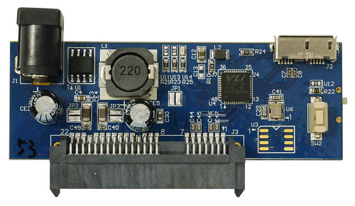
VIA Labs links USB3.0 to SATA
V bridge controller provides more flexibility for embedded designs
By Nick Flaherty www.flaherty.co.ukEmbedded chip developer VIA Labs has had its VL701 Low-Power USB 3.0 to SATA Bridge Controller certified by the USB Implementers Forum (USB-IF) as adhering to strict power-consumption criteria for bus-powered devices. VIA Labs is currently the first and only company to achieve USB-IF Bus-Powered certification using a traditional hard disk drive, which draws more power than flash-based devices.
The comprehensive suite of tests conducted as part of the USB-IF Compliance and Certification Program ensures that certified products are interoperable with existing USB devices while also offering all the speed and power enhancements of the USB 3.0 specification.
With the industry's first fully-integrated 5V switching regulator, the VL701 is a highly integrated single chip solution that allows users to connect any SATA hard disk drive (HDD), solid state drive (SSD), or optical disc drive (ODD) to their PC via USB 3.0. With data transfer rates of up to 5Gbps, data stored on SATA devices can be effortlessly transferred to a PC in a fraction of the time it would usually take compared to USB 2.0 or Firewire.
Cal-Comp Electronics and Communications, a leading Electronics Manufacturing Services (EMS) and Original Design Manufacturer (ODM) that contracts with many name-brand customers worldwide, adopted and integrated the USB-IF Certified VL701 it into its upcoming USB 3.0 external storage products.
“The VL701 is an advanced, highly-integrated USB 3.0 to SATA Bridge that lets users experience the benefits of USB 3.0 using hard drives, optical drives, and even SSDs,” said David Hsu, Associate Vice President, VIA Labs, Inc. “The low power aspect is compelling for both end-users and manufacturers by enabling lower operating temperatures and longer battery life without sacrificing performance.”
Related articles
- Intel's Ivy Bridge chipset in 2012, will support both Thunderbolt and USB 3.0 (geek.com)
- Intel Calls USB 3.0 & Thunderbolt 'Complementary,' Will Support USB 3.0 in 2012 (crunchgear.com)
- Plextor Taps USB 3.0, eSATA For The PX-LB950UE, 12x External Blu-ray Writer (crunchgear.com)
- AMD Opens up USB 3.0 for PCs With Chipset Support (pcworld.com)
Portable Multimedia: NVIDIA makes key move into wireless with Icera
NVIDIA is to add baseband and RF capability to its Tegra processors by acquiring reconfigurable technology developerIcera in a $367m deal.
“This is a key step in NVIDIA’s plans to be a major player in the mobile computing revolution,” said Jen-Hsun Huang, President and CEO of NVIDIA. “Adding Icera’s technology to Tegra gives us an outstanding platform to support the industry’s best phones and tablets."
NVIDIA is to add baseband and RF capability to its Tegra processors by acquiring reconfigurable technology developerIcera in a $367m deal.
“This is a key step in NVIDIA’s plans to be a major player in the mobile computing revolution,” said Jen-Hsun Huang, President and CEO of NVIDIA. “Adding Icera’s technology to Tegra gives us an outstanding platform to support the industry’s best phones and tablets."
Related articles
- NVIDIA snaps up software baseband maker Icera (arstechnica.com)
- NVIDIA and ICERA Create Serious Competition for Qualcomm and Others (slashgear.com)
- Nvidia Buys Phone Chip Maker (online.wsj.com)
- NVIDIA Sets Its Sights on Qualcomm (fool.com)
- Why all mobiles and tablets uses Nvidia Tegra Chipsets (techdraginfo.blogspot.com)
- Nvidia Outlines Plan To Attack Computing Market, Shares Fall Amidst Worries About Competition (blogs.forbes.com)
BVM brings the Core i7/i5/i3 to industrial applications in Mobile MicroATX
By Nick Flaherty www.flaherty.co.uk
BVM in Southampton has added to its family of compact Micro ATX format motherboards with a motherboard based on Intel's Mobile QM57 Express chipset. This allows the MS-C71 to support the 32nm Intel Core i7/i5/i3 Mobile processors in the rPGA988A socket with up to 8GB of 1066MHz dual-channel memory to minimise power consumption and reduce the cooling requirements of the finished system. Typical applications will be in kiosks, large-scale displays, industrial control and automation, security and surveillance, gaming, print imaging, digital signage and other applications where fast processing is a fundamental requirement.
HD audio is provided by the Realtek ALC888 HD Audio codec; HD VGA, 24-bit dual channel LVDS and optional DVI video are supported. Twelve USB2.0, five RS232 and one RS232/422/485 serial ports, two Gigabit Ethernet RJ45 network ports and an S/PDIF audio port are onboard. For mass storage, six ATA II 300MB/s interfaces supporting RAID 0/1/5/10 are provided. Expansion capability includes PCI-Express X16 and X4 slots, two PCI slots, one Mini-PCIe and oneMini-PCI sockets and a Compactflash socket.
Power is from any standard 24-pin ATX PSU, with onboard ACPI 2.0 compliant power management. A programmable 8-bit digital I/O interface, real time clock and watchdog timer also come as standard features.
Related articles
- Is Micro ATX The Standard For The Masses? (lockergnome.com)
- Finding the Best Motherboard for Your HTPC Project (brighthub.com)
- Motherboard Buying Guide (brighthub.com)
Monday, May 09, 2011
Broadcom to add security software to embedded systems with Israeli acquisition
By Nick Flaherty www.flaherty.co.uk
Following the trend set by Intel's acquisition of anti-virus software developer McAfee, Broadcom is to acquire a leading security software developer based in Israel.
With SC Square Ltd., Broadcom is acquiring an expert team of engineers focused on security, which Broadcom says is an essential ingredient across its embedded platforms. The acquisition is part of Broadcom's strategy to acquire innovative technologies and high quality teams with a solid track record of execution.
In connection with the acquisition, Broadcom expects to pay approximately $41.9m in cash to acquire all of the outstanding shares of capital stock and other equity rights of SC Square.
.. as the board adds new (ish) faces
Long term Broadcom chief technology officer and co-founder Dr Henry Samueli is to re-join the board of the company after a three year break and after a lawsuit over the backdating of share options was settled last month.
Dr. Samueli, who co-founded Broadcom in 1991, previously served on Broadcom's Board as Co-Chairman from April 1998 to May 2003 and as Chairman from May 2003 to May 2008.
He is joined by Dr. Maria Klawe, President of Harvey Mudd College, a private liberal arts college in Claremont, Calif., whose focus is on engineering, science and mathematics. Prior to joining Harvey Mudd, she served as Dean of Engineering and Professor of Computer Science at Princeton University from 2003 to 2006. From 1988 to 2002, she held several positions at the University of British Columbia including Dean of Science, Vice President of Student and Academic Services and head of the Department of Computer Science. She has also worked at IBM Research in California, the University of Toronto and Oakland University in Michigan. Dr. Klawe received her bachelor's degree and doctorate in mathematics from the University of Alberta, Canada. "The addition of these two eminent technologists, educators and innovators to our Board will serve Broadcom well for years to come," said Scott McGregor, Broadcom's president and chief executive officer. "Henry has been instrumental in developing and implementing Broadcom's innovation and technology strategy which has catapulted the company to its leadership position in semiconductors for wired and wireless communications," McGregor said. "Dr. Klawe is also an important addition to our Board given the critical importance to our business of scientific and engineering innovation. Dr. Klawe's understanding of scientific research and the science, technology, engineering and math (STEM) talent pipeline, as well as her experience in the management and operations of large organizations will be invaluable to our Board."
Related articles
- Is Broadcom Working Hard Enough for You? (fool.com)
- Broadcom beats 1Q views, but outlook disappoints (seattlepi.com)
- Techs edge up, but Broadcom shares tumble (marketwatch.com)
- Broadcom Co-Founders Settle Shareholder Backdating Lawsuit (businessweek.com)
Friday, May 06, 2011
Logic PD claims world's smallest embedded system-on-module
Based on TI's DaVinci digital media processor and Sitara ARM microprocessor
By Nick Flaherty www.flaherty.co.uk
Logic PD has launched what it claims is the industry’s smallest embedded modules: the Torpedo System on Modules (SOM) based on Texas Instruments’ DM3730 DaVinci video processor and AM3703 Sitara ARM microprocessor.
By Nick Flaherty www.flaherty.co.uk
Logic PD has launched what it claims is the industry’s smallest embedded modules: the Torpedo System on Modules (SOM) based on Texas Instruments’ DM3730 DaVinci video processor and AM3703 Sitara ARM microprocessor.
The Torpedo SOMs (above) occupy less than one square inch yet offer the highest performance and lowest power consumption in the market with fast product development and enable companies to further condense hardware space requirements while increasing overall system performance.
“Logic PD’s long-standing relationship with Texas Instruments and our vast system design experience enable us to deliver this unique balance of size, speed and processing power,” said Kurt Larson, director of product management at Logic PD. “Our modules reduce design complexity and time to market allowing users to create market changing products ahead of their competition.”
The DM3730 and AM3703 Torpedo SOMs are less than one square inch in size and provide PC-like speeds up to 1GHz with long battery life with power consumption of less than 5 mW in suspend state. The ultra-compact Torpedo SOMs are an ideal off-the-shelf solution for applications in markets where space is a premium, such as point-of-care medical devices, handheld radios and mobile Internet devices.
Like the Torpedo SOMs, the DM3730 SOM-LV and AM3703 SOM-LV are based on Texas Instruments’ DM3730 DaVinci video processor and AM3703 Sitara ARM microprocessor, and provide speeds up to 1 GHz and low power consumption. In a slightly larger form factor, Logic PD’s DM3730 SOM-LV also offers on-board Wi-Fi (802.11b/g/n) and Bluetooth 2.1 + EDR wireless radios, and a 10/100 Ethernet controller. The AM3703 SOM-LV provides a lower cost option that includes the Ethernet controller for network connectivity but no wireless features. The SOM-LV products are ideal for applications in the medical, point-of-sale, industrial and security markets, such as patient monitoring, bar code readers and CCTV cameras.
Logic PD provides Android, Linux and Windows CE board support packages (BSPs) for use with all versions of the DM3730 and AM3703 SOMs. These BSPs are designed, developed and tested using an ISO 13485 certified process to ensure quality and reduce risk. Additionally, by maintaining footprint compatibility with Logic PD’s existing OMAP35x SOM product lines, the DM3730 and AM3703 SOMs extend the longevity of existing products through drop-in performance improvements while maintaining scalability to future technologies.
“By combining our high-performance Sitara ARM microprocessors and DaVinci video processors with Logic PD’s design expertise, the new AM3703 and DM3730 SOMs ease product development and reduce overall design complexity by removing the 0.4 mm package and memory routing issues many customers face. In turn, this allows our customers the ability to bring fast, high-performance hardware and software to market sooner,” said Juan Gonzales, DM3730 DaVinci video processor marketing manager at Texas Instruments.
Pricing & Availability
Logic PD’s Zoom DM3730 Torpedo Development Kit and Zoom DM3730 SOM-LV Development Kit, including Wattson, a power measurement and performance monitoring application, will be available in June and July, respectively, through Logic PD distributors. The suggested retail price is $997. For SOM pricing and for more information, contact product.sales@logicpd.com.
“Logic PD’s long-standing relationship with Texas Instruments and our vast system design experience enable us to deliver this unique balance of size, speed and processing power,” said Kurt Larson, director of product management at Logic PD. “Our modules reduce design complexity and time to market allowing users to create market changing products ahead of their competition.”
The DM3730 and AM3703 Torpedo SOMs are less than one square inch in size and provide PC-like speeds up to 1GHz with long battery life with power consumption of less than 5 mW in suspend state. The ultra-compact Torpedo SOMs are an ideal off-the-shelf solution for applications in markets where space is a premium, such as point-of-care medical devices, handheld radios and mobile Internet devices.
Like the Torpedo SOMs, the DM3730 SOM-LV and AM3703 SOM-LV are based on Texas Instruments’ DM3730 DaVinci video processor and AM3703 Sitara ARM microprocessor, and provide speeds up to 1 GHz and low power consumption. In a slightly larger form factor, Logic PD’s DM3730 SOM-LV also offers on-board Wi-Fi (802.11b/g/n) and Bluetooth 2.1 + EDR wireless radios, and a 10/100 Ethernet controller. The AM3703 SOM-LV provides a lower cost option that includes the Ethernet controller for network connectivity but no wireless features. The SOM-LV products are ideal for applications in the medical, point-of-sale, industrial and security markets, such as patient monitoring, bar code readers and CCTV cameras.
Logic PD provides Android, Linux and Windows CE board support packages (BSPs) for use with all versions of the DM3730 and AM3703 SOMs. These BSPs are designed, developed and tested using an ISO 13485 certified process to ensure quality and reduce risk. Additionally, by maintaining footprint compatibility with Logic PD’s existing OMAP35x SOM product lines, the DM3730 and AM3703 SOMs extend the longevity of existing products through drop-in performance improvements while maintaining scalability to future technologies.
“By combining our high-performance Sitara ARM microprocessors and DaVinci video processors with Logic PD’s design expertise, the new AM3703 and DM3730 SOMs ease product development and reduce overall design complexity by removing the 0.4 mm package and memory routing issues many customers face. In turn, this allows our customers the ability to bring fast, high-performance hardware and software to market sooner,” said Juan Gonzales, DM3730 DaVinci video processor marketing manager at Texas Instruments.
Pricing & Availability
Logic PD’s Zoom DM3730 Torpedo Development Kit and Zoom DM3730 SOM-LV Development Kit, including Wattson, a power measurement and performance monitoring application, will be available in June and July, respectively, through Logic PD distributors. The suggested retail price is $997. For SOM pricing and for more information, contact product.sales@logicpd.com.
Related articles
- Cortex-A8 modules are 'industry's smallest' (linuxfordevices.com)
- OMAP-ready 720p camera module offers low-light sensitivity (linuxfordevices.com)
Renesas moves mobile chip to SODIMM modules for embedded apps
Works with Cogent on system-on-module
By Nick Flaherty www.flaherty.co.ukRenesas Electronics has teamed up with Cogent Computer Systems to puts its SH-Mobile SH7724 chip onto a System On Module (SOM) for low cost, rapid development of embedded systems.
The SH-Mobile R-Series is an application processor based on Renesas SH-Mobile series, which is widely used in mobile phones in Japan and other countries. It was developed to allow advanced multimedia functions of the SH-Mobile device such as camera processing, and video and audio processing, to be applied in fields other than mobile phones.
The processor incorporates multi-codec, high-performance video processing IP supporting the H.264/MPEG-4 AVC (H.264) video compression standard used by ISDB-T terrestrial digital broadcasts in Japan, as well as the One-Seg format used for terrestrial digital broadcasts in Europe, China and other regions. To support playback and recording of HD (high definition, 1280 × 720 pixels) video, functionality is provided for encoding (recording) and decoding (playback) of HD-format video at 30 frames per second (fps). Also, the operating frequency of 500MHz provides power to spare when running a general-purpose operating system (OS) such as Linux.
In addition to the these features, camera input has been increased to two channels and an Ethernet MAC (Media Access Control) supporting data transfer at 10/100 megabits per seconds (Mbps) has been newly added. This extends the range of suitable applications beyond low-end navigation systems, where Renesas Electronics’ application processors already have an extensive track record, to include IP security cameras, videoconferencing systems, video and voice over IP (V2IP), networked household appliances, drive recorders, digital signage, etc.
Cogent’s CSB765 SOM module provides more time, at less cost and less risk, for engineers to create their unique products, based on the proven Renesas Electronics SH-Mobile SH7724 applications processor.
The GPIO and peripherals are made available via the low cost 200-pin SODIMM edge connector.
In addition to the these features, camera input has been increased to two channels and an Ethernet MAC (Media Access Control) supporting data transfer at 10/100 megabits per seconds (Mbps) has been newly added. This extends the range of suitable applications beyond low-end navigation systems, where Renesas Electronics’ application processors already have an extensive track record, to include IP security cameras, videoconferencing systems, video and voice over IP (V2IP), networked household appliances, drive recorders, digital signage, etc.
Cogent’s CSB765 SOM module provides more time, at less cost and less risk, for engineers to create their unique products, based on the proven Renesas Electronics SH-Mobile SH7724 applications processor.
The GPIO and peripherals are made available via the low cost 200-pin SODIMM edge connector.
Specifications
- 500MHz SH-4A superscalar core (900 DMIPS) with 32 KB I-cache/32 KB D-cache
- 256KB L2 cache and 128KB on-chip high-speed media SRAM
- IEEE754-compliant single-/double-precision FPU (3.5GFLOPS)
- 128MB low-power mobile LPDDR-333 SDRAM
- 64MB S29GL512N flash, with secure 256 byte sector and 128-bit unique ID
- On-chip LCD controller up to 1280 x 720 pixels with 2D graphics, scaling and rotation
- Hardware video decoding up to 720P, MPEG-4, H.264, JPEG and WMV
- 8bit video-input port supporting YUV4:2:2, CCIR656 and CMOS sensors up to 5MP
- Sound processing unit with dual 24-bit MAC DSP, 160KB program and 264KB data RAM
- High-speed (480MBit) USB 2.0 OTG port and USB host port
- On-chip 10/100Mbit Ethernet controller
- DS1339 real-time clock with dedicated battery backup input
- 2-wire RS-232 debug serial port plus three 2-wire TTL UARTS (with GPIO handshaking)
- I2S, SPI (x2) and I2C (x2) for I/O expansion such as touch, audio, A/D, D/A, etc.
- Dual SD/MMC controllers (4-bit, SDIO-compliant)
- Buffered 25-bit address/16-bit data bus for generic expansion
- 10 dedicated GPIO (may also carry some CPU functions)
- On-board, wide input (6V to 24V) 3.3V regulator provides 3A to the target board
- <750mw typical, 1500mw maximum, <20mw sleep to RAM
Pricing and Availability
More information about the CSB765 SOM can be found at www.cogcomp.com/csb_csb765.htm. For pricing and availability, contact NuHorizons http://www.nuhorizons.com/.
Related articles
- Chip Maker Renesas Is Running at Half-Speed (online.wsj.com)
- RSODIMM: a low-cost way to make SODIMMs rugged (linuxfordevices.com)
- Report: Renesas Electronics to restart automotive microchip production early (autoblog.com)
- Japan's Renesas to restart key plant early: report (marketwatch.com)
- Renesas Looks to Bring Two Factories Back Online (online.wsj.com)
- Japan's Renesas says working to bring forward factory re-start (reuters.com)
- After The Quake, Chip Maker Renesas Runs at Half Speed [Voices] (voices.allthingsd.com)
- Japan Renesas restarts production at Yamagata factory (reuters.com)
Microchip moves to Open-Source development tool with full cross-platform support
MPLAB X IDE adds multiple simultaneous debugging sessions, advanced editor and code completion for Linux, Mac and Windows
By Nick Flaherty www.flaherty.co.uk
Microchip, one of the leading suppliers of 8, 16 and 32bit microcontrollers, has launched its next-generation, open-source Integrated Development Environment (IDE) based on Netbeans with cross-platform support for Linux, Mac OS and Windows operating systems.
By Nick Flaherty www.flaherty.co.uk
Microchip, one of the leading suppliers of 8, 16 and 32bit microcontrollers, has launched its next-generation, open-source Integrated Development Environment (IDE) based on Netbeans with cross-platform support for Linux, Mac OS and Windows operating systems.
The new MPLAB X IDE introduces the ability to manage multiple projects and tools with simultaneous debugging, an advanced editor, visual call graphs and code completion. MPLAB X is also unique in the industry due to its support for a complete portfolio of 8, 16 and 32bit microcontrollers, including all 800+ PIC microcontrollers, dsPIC digital signal controllers and memory devices. This gives the designer a large amount of flexibility to get the right controller mapped to the embedded application.
MPLAB X provides a single, unified graphical interface for Microchip and third-party tools, including the MPLAB ICD 3, PICkit 3 and MPLAB REAL ICE debugger/programmers.
It builds on the core benefits of the Oracle Sponsored open-source NetBeans platform which has an active user community that can contribute a wide range of enhancements and third-party plug-ins. Microchip customers can also take advantage of free NetBeans software components and plug-ins that are available immediately, as well as the capability to customise MPLAB X IDE to match individual development needs.
Additional features include:
MPLAB X provides a single, unified graphical interface for Microchip and third-party tools, including the MPLAB ICD 3, PICkit 3 and MPLAB REAL ICE debugger/programmers.
It builds on the core benefits of the Oracle Sponsored open-source NetBeans platform which has an active user community that can contribute a wide range of enhancements and third-party plug-ins. Microchip customers can also take advantage of free NetBeans software components and plug-ins that are available immediately, as well as the capability to customise MPLAB X IDE to match individual development needs.
Additional features include:
- Import utility for quick and easy migration of projects from the previous MPLAB IDE platform
- Code completion and context menus via advanced editor
- Configurable watch window
- Supports multiple compiler versions, simultaneously
- Team collaboration tools for bug tracking and source-code control
The MPLAB X IDE can be explored via a free download at: http://www.microchip.com/get/D413, and users can provide feedback via the MPLAB X Users’ Forum at http://www.microchip.com/get/M6RA.
Subscribe to:
Posts (Atom)