Despite the collapse of the new car market, iSuppli is predicting a boom in telematics equipment for vehicles in Western Europe over the next ten years, and the details of the usage of telematics for each brand make very interesting reading (below), particularly the relatively low levels of telematics used today.
Sales of automotive telematics systems are set to rise by a factor of five during the period from 2008 to 2016 as carmakers offer more telematics-equipped models in the region, reaching 24.8 million systems by 2016, expanding at a Compound Annual Growth Rate (CAGR) of 22.5 percent from 4.9 million systems last year.
“Automotive telematics is defined as the integrated use of telecommunications and informatics, allowing the sending and receiving of information,” said Anna Buettner, analyst for automotive electronics at iSuppli. “Telematics can provide a range of benefits to motorists, from notifying an emergency operator when a car’s airbags have been deployed, to reporting vehicle conditions to a remote monitoring center.”
Two major types of telematics solutions are being offered on the market: embedded systems, whose functionality is integrated into the headunit of cars; and mobile-device oriented systems, which use a wireless product like a cell phone to communicate information.
“iSuppli believes that embedded and mobile-device-based telematics systems will continue to coexist in the car market in Western Europe and elsewhere,” Buettner said. “Embedded solutions are suitable for high-end luxury models, while mobile-device-oriented systems can bring telematics services to high-volume, entry-level cars. Regardless of which approach is used, pipes used for communications and delivery of content will become increasingly transparent and will be modified to cater to a vast array of data types.”
GM’s telematics sales in Western Europe are projected to grow to more than 1.4 million units in 2016, rising at a CAGR of more than 41 percent from 210,000 million in 2008. GM currently offers only mobile-device-based telematics systems.
Ford is expected to introduce the Sync system in Europe in 2011. This should increase its mobile-device telematics system shipments in the region to more than 1.7 million systems in 2016, rising at a Compound Annual Growth Rate (CAGR) of 31 percent from 190,000 in 2008.
The Japanese brands are not as strong in Europe as they are in North America, so their telematics sales will be much lower in the region. Toyota, which maintains the largest auto sales among the Japanese brands in Western Europe, will have the highest telematics sales there—growing to 990,000 units in 2016, up at a CAGR of 31 percent from 110,000 in 2008. The Japanese leader most likely will bring an embedded solution to the market in the near future.
Domestic telematics
The Top-6 European auto manufacturers collectively control about 64 percent of the Western European auto market.
PSA now has the highest telematics sales in Europe due to its use of both embedded and mobile-device systems. Company sales are forecasted to grow to 3.1 million systems in 2016, up from nearly 620,000 in 2008. Embedded systems accounted for 42 percent of PSA’s 2008 telematics sales.
VW’s telematics sales are projected to grow to nearly 3.2 million units in 2016, increasing at a CAGR of more than 26 percent from 490,000 systems in 2008. While the company’s four brands currently use only mobile device telematics systems, the German OEM is expected to introduce an embedded telematics system in the future.
Fiat’s three brands will sell 2.3 million units in 2016, up at a CAGR of 27 percent from 340,000 in 2008. Embedded systems accounted for about 20 percent of Fiat’s telematics sales in 2008.
Renault has been slow to adopt telematics and has just recently added mobile device systems. Renault’s telematics sales are projected to grow to 1.6 million units in 2016, rising at a CAGR of 30 percent from 190,000 in 2008.
The two main luxury brands in Europe, BMW and Mercedes-Benz, already sell a high percentage of their autos with telematics systems.
BMW uses both embedded and mobile device telematics systems. Company telematics sales will rise to more than 1.3 million units in 2016, up at a CAGR of 16 percent from 390,000 in 2008.
Mercedes-Benz currently sells only mobile-device telematics systems. Sales of Mercedes-Benz telematics systems are forecasted to grow to 1.4 million systems in 2016, expanding at a CAGR of almost 20 percent from 320,000 in 2008. Similar to Toyota/Lexus and Volkswagen, Mercedes-Benz also is expected to introduce an embedded telematics solution for its future offerings.

Wednesday, November 11, 2009


Cognitive radio for old TV spectrum

Cambridge Consultants has developed a novel, low-cost ‘spectral sensing’ cognitive radio technology platform that will allow any radio product to transmit without interference over so the called ‘whitespace’ frequencies at 700MHz recently vacated by the US digital TV switchover. With InCognito, it is aiming to do for whitespace what it did for Bluetooth and Zigbee, spinning off companies such as Cambridge Silicon Radio.
Whitespace is highly desirable TV band frequencies that easily penetrate walls, potentially extending the range of Home Area Networks (HANs) and enabling a range of novel new applications, such as reliable high-definition video streaming from a single access point to every room in a house. Innovative use of whitespace radio will also make it possible to increase the accessibility of low-cost high speed wireless internet services, including those rural communities which are currently poorly served.
The new frequencies, recently authorised in the USA by the Federal Communications Commission (FCC), greatly increase the overall wireless bandwidth available to computers, set top boxes, laptops, WiFi hot spots and other radio devices that currently use the unlicensed band around 2.4GHz. They also have the potential to greatly extend the range of these devices.
“We’ve seen so much game-changing innovation in the unlicensed 2.4GHz band, but I believe the FCC’s decision to open up the ‘whitespace’ radio frequencies for innovation promises even more. We will quickly see a wave of innovation in wireless products and services around 700MHz, bringing benefits both to consumers and to the innovative businesses that move quickly into the whitespace market,” said Luke D’Arcy of Cambridge Consultants.
But the decision is not without controversy. The primary incumbent users of these TV band frequencies are concerned about the potential for interference caused by the influx of new users. “Based on highly complex cognitive ‘spectral sensing’ radio technology which, until now, has only been used in defence and security applications, the InCognito platform enables ‘whitespace’ radios to quickly and accurately detect and avoid other broadcasts," saidD'Arcy. "We also understand that the most successful technologies in use in these markets today are based on open industry standards, which is why we have taken our platform to the CogNeA Alliance. This, together with our track record of fast product development, means that any client can take advantage of the new spectrum quickly and easily - adding this potentially low cost technology to a client’s device could take as little as a few months. I believe we will start to see the first cognitive radio enabled products in mid 2010 and that the market will develop quickly.”
The CogNeA Alliance aims to drive the definition and adoption of industry-wide standards for wireless devices to operate over the new TV white spaces. Kiran Challapali, CogNeA’s Chairman, said “Cambridge Consultants has helped get many successful new standards such as Bluetooth, DECT and Zigbee off the ground. We welcome them to our alliance, which includes companies like Philips, Samsung Electro-Mechanics, ETRI and Georgia Tech, and we look forward to working together to make CogNeA a successful standard."
Intel moves into equipment with the Reader

Intel's Digital Health group has launched a handheld device in the US that reads out text. This is one of the few times that Intel has sold consumer equipment under its own brand and is a key step towards the Intel phone. Intel already makes notebooks and netbooks, but these are all labelled by, and sold by, other companies.
The Intel Reader is designed to increase independence for people who have trouble reading standard print. About the size of a paperback book, it converts printed text to digital text, and then reads it aloud to the user. It combines a high-resolution camera with an Intel Atom processor, allowing users to point, shoot and listen to printed text.
The original concept for the Reader came from Ben Foss, a researcher at Intel who was identified in elementary school as one of the estimated 20 percent of people nationwide who have symptoms of dyslexia. Throughout high school, college and graduate school, he had to depend on others to read to him or work through the slow process of getting words off of a page himself. As an adult, much of the content he wanted, from professional journals to pleasure reading, just wasn't available in audio form.
"As someone who is part of this dyslexic community, I am thrilled to be able to help level the playing field for people who, like me, do not have easy access to the printed word," said Foss. "Feelings of loneliness are often the experience of not being able to read easily. We hope to open the doors for people in these communities. The Intel Reader is a tool that can help give people with dyslexia, low-vision, blindness or other reading-based disabilities access to the resources they need to participate and be successful in school, work and life."
Intel says it can assist the estimated 55 million people in the U.S. who have dyslexia or other specific learning disabilities, or have vision problems such as low-vision or blindness, which makes reading printed words difficult or impossible.
The Intel Reader will be available in the United States through select resellers, including CTL, Don Johnston Incorporated, GTSI, Howard Technology Solutions and HumanWare.
When the Intel Reader is used together with the Intel Portable Capture Station, large amounts of text, such as a chapter or an entire book, can be easily captured for reading later. It is available through selected outlets in the US.
"The Intel Digital Health Group's expertise is in finding innovative technology solutions to improve quality of life," said Louis Burns, vice president and general manager of Intel's Digital Health Group. "We are proud to offer the Intel Reader as a tool for people who have trouble reading standard print so they can more easily access the information many of us take for granted every day, such as reading a job offer letter or even the menu at a restaurant."
Monday, November 02, 2009
DDR3 memory - what happend?

I've just had to buy a new laptop, and wanted something that would last for a good few years, so naturally wanted high speed, low power DDR3 memory. Could I find much? No, really just Dell and Acer.
So this analysis of what happened from Malcolm Penn at Future Horizons is well timed, and an excellent description of how technology does, or doesn't get adopted, and the implications for the embedded market! It looks like my timing is good though as now I have a lovely DDR3 system at a reasonable, not bleeding edge, cost.
Semiconductor Spotlight – DDR3
The DRAM manufacturers as a whole made a combined loss during 2008 of US$20 billion. At the moment memory pricing is firming but semiconductor memories are still plagued by a regular cyclicality of over-capacity and declining ASPs countered by tightening capacity and rising ASPs. However, although improvements are evident in the short term, the longer-term trends are still up for debate. One of the major trends currently under way is the trend to DDR3 memory from the current mainstream DDR2.
DDR, DDR2 and DDR3 are types of SDRAM (Synchronous Dynamic Random Access Memory) and use a clock signal for synchronization. DDR stands for Double Data Rate, meaning that memories from this category transfer two data chunks per clock cycle.
One of the main differences between DDR, DDR2 and DDR3 is the highest transfer rate each generation can achieve. For example, higher speed DDR2-1066 memory operates at a clock rate of 533 MHz. Whilst there is an equivalent DDR3 memory that also operates at this speed, the DDR3-1600 operates with a clock rate of 800MHz. In addition, the internal data path of DDR2 memory is 4 bits whilst DDR3 is 8 bits. DDR3 memories also operate at lower voltages compared to DDR2 memories.
This lower voltage means that DDR3 consumes less power than DDR2 for a given clock rate and lower power is becoming increasingly important for laptops and the general trend of electronic equipment to become ‘greener’.
On the minus side, DDR3 memories have higher latencies than DDR2 memories. This means that DDR3 memories take more clock cycles initially before delivering data compared to DDR2 memories.
The primary benefit of DDR3 is the ability to transfer at twice the data rate of DDR2. DDR3 can operate at higher clock rates than DDR2 and DDR3 memory uses less power for the same clock rate. An emphasis on low power and higher data rates make DDR3 memory a more attractive option provided there is a low premium on price and the motherboards are ‘DDR3 ready’.
The first DDR2's replaced DDR in PCs by Dell during the summer of 2004 and were DDR2-533 specification. Dell has been one of the leaders in new system development and it was expected that that the transition to DDR2 would start getting underway very soon after. However, history showed that the uptake of DDR2 was not a smooth transition with memory manufacturers reverting to DDR and then going back to DDR2. The changeover eventually occurred during early 2006 when DDR2-667 had both a performance and price advantage.
It looks as though history will repeat itself with the transition to DDR3 from DDR2 but perhaps over a shorter time-span. DDR3 has been in gestation since 2005 and has appeared on some motherboards during 2007. Optimistic predictions were made for adoption during early 2008 with predictions of 30 percent or more penetration of DDR3 memory with less than ten percent price difference in price over DDR2 by the end of 2008.
By mid-year 2008 this prediction was looking increasingly unlikely and eventually did not happen. However, the pricing has been altering in favour of DDR3 in the last four months and the percentage of DDR3 has been creeping up to over 20 percent of total PC memory in the first half of this year.
PC OEMs are inexorably price driven and will tend to use the cheapest available memory given comparable performance in mainstream machines. Another factor is, of course, the type of memory the motherboard can take. DDR3 has become more popular since July and, as a consequence, the price for this memory rose as demand increased.
As the DDR3 prices increased, PC manufacturers started to go back to using DDR2 as these were lower in price. However, increased DDR2 demand, in turn, drove up prices. With prices now higher for DDR2, PC OEMs will switch back to DDR3 parts. This cycle will likely continue for the next six months until DDR3 memory becomes the mainstream memory for PCs probably during mid-2010.
The adoption of any new technology is always beset by problems in its introduction and the transition from DDR2 to DDR3 is promising to be no exception. It has been clear for some time that DDR3 memory has had the potential to become the mainstream PC memory but market adoption depends on a careful mix of price and performance with a lot of emphasis on price.
As such we believe DDR3 will really come into its own when the new generation 50nm designs hit the market. This advance will also allow a large increase in die-per-wafer and either an improvement in profitability or a tool to increase market share depending on the individual memory manufacture’s strategy.
China supercomputer breaks performance barrier

China's National University of Defense Technology (NUDT) has developed a supercomputer that breaks the petaflop barrier, putting China in the same league as the US and Europe for high performance computing.
The supercomputer, called "Tianhe", meaning Milky Way, is based in Changsha, capital of central China's Hunan Province.
The 155-ton system, with 103 refrigerator-like cabinets covering an area of about 1,000 square meters cost $88m and is expected to process seismic data for oil exploration, conduct bio-medical computing and help design aerospace vehicles. It uses 6,144 Intel CPUs and 5,120 AMD GPUs, and reaches a peak performance of 1.206 petaflops and 563.1 teraflops on the Linpack benchmark, making it currently the fourth most powerful machine on the planet.
China's Dawning Information Industry Company is attempting to build its own supercomputer that overcomes the petaflop barrier by 2010, and the NUDT is planning to add "hundreds or thousands of China-made CPUs" to the machine to improve its Linpack performance to over 800 teraflops.
Tuesday, October 20, 2009
Ultra low power microcontroller extends battery life


A Norwegian startup is pushing the limits of low power in microcontrollers, cutting power by a factor of four over even 8bit devices.
Energy Micro has developed the EFM32 low power 32bit microcontroller based on the ARM Cortex-M3 architecture with low power clocks and peripherals that consumes less than 180µA per MHz while executing real life code from Flash memory and the lowest active mode current consumption of any microcontroller. Its standby current consumption is also the lowest, at typically 900nA while running real time clock, power-on reset, brown-out detector and full RAM and CPU retention and less than 20nA in its deepest sleep mode. The start-up time of less than 2µs is also the industry’s fastest. The power is lower than traditional 16 or 8bit devices from Silicon Labs, Texas Instruments and Microchip (see chart).
“We are very proud that we have delivered on our mission to provide the world with the most energy friendly microcontrollers,” said Geir Forre, founder and CEO. “By introducing innovative new energy saving features, such as our peripheral reflex system and energy management unit, the potential saving in battery life that can be achieved is immense.”
The low power peripherals include:
a 4x40 segment LCD controller running at less than 900nA;
an 8-channel 12-bit 1M samples/sec ADC running at less than 200µA;
a brown-out detector running at less than 100nA;
a 32kHz real time counter running at 50nA;
and a UART capable of 9600bps at 100nA.
The devices, built in standard low leakage CMOS, are initially targetted at smart metering and home automation, with battery lifetimes of 10 to 15 years with low cycle times. “The EFM32G family of microcontrollers has been specified in close partnership with many world leading companies within, for example, the energy metering, home and building automation and alarm and security industries,” said Øyvind Janbu, co-founder and CTO of Energy Micro. “Working so closely with top engineers in such sectors has enabled us to produce a family of microcontrollers that truly is a perfect fit for a variety of different applications.”
One of Energy Micro’s partner customers is window maker Velux, one of the strongest brands in the global building materials and home improvement industry. It is planning to use the EFM32 in a range of contorllers later this year.
Meter company Kamstrup is also looking to use the device for products next year.
There are 22 different EFM32G microcontroller products which will become available over the next few months, in a variety of packages including QFN32, QFN64, QFP100 and BGA112. The EFM32G operates from a single supply rail of between 1.8 and 3.8V. The operating temperature range is –40degC to +85degC. The microcontrollers provide up to 128KB Flash memory and up to 16KB of RAM.
The first products are being offered by Energy Micro in QFN64 and BGA112 profiles and are currently sampling with lead customers. Pricing for the initial 32-pin devices starts at $1.55 in 100k quantities.
Friday, October 16, 2009
Virage aims for IP powerhouse with NXP deal
So, Virage Logic is taking another step towards becoming a major IP and system on chip player with a deal to acquire key IP from NXP.
The deal sets up an R&D centre for Virage in Eindhoven, home of NXP, for advanced CMOS I/O, analogue mixed signal and System-on-Chip (SoC) infrastructure IP. These new products are expected to be commercially available in early 2011, and sit alongside the UK-based ARC configurable processor technology acquired in August this year, creating an SoC powerhouse.
Under the terms of the multi-year agreement, NXP will transfer over 160 employees and the assets associated with selected advanced CMOS libraries, IP blocks and SoC architecture along with other classes of semiconductor IP, including approximately 25 associated patent families. In return, NXP will receive 2.5 million shares of Virage Logic common stock and a share of the future revenue generated by Virage Logic from licensing the transferred IP portfolio. In addition, Virage Logic will provide to NXP services surrounding the transferred IP for a 3.5-year period, and NXP will receive a 3.5 year license to Virage Logic’s extensive standard-products semiconductor IP portfolio for all future SoC designs.
For all of this, NXP pays $60m over the next four years!
Dan McCranie, executive chairman for Virage Logic, said, “Over two years ago, we embarked on a transformation that was based on several key strategic initiatives. Amongst those initiatives were, a) the broadening of our IP product portfolio through both organic and inorganic growth and, b), establishing Virage Logic as the semiconductor industry’s Trusted IP partner. Today’s announcement with NXP represents strong progress on both of those initiatives. All of us at Virage Logic are proud of the confidence that NXP has shown in our technical teams to be selected as the IP provider to NXP for their future development. In addition, we are excited about the future ability to expand our IP offerings to the semiconductor industry through the productizing of NXP’s important IP elements.”
“Virage Logic was founded on the vision that an independent IP company could provide the technically superior building blocks the global semiconductor industry needs to develop their highly differentiated end products more cost effectively and deliver them to market more quickly,” said Dr. Alex Shubat, president, CEO and co-founder of Virage Logic.
The deal sets up an R&D centre for Virage in Eindhoven, home of NXP, for advanced CMOS I/O, analogue mixed signal and System-on-Chip (SoC) infrastructure IP. These new products are expected to be commercially available in early 2011, and sit alongside the UK-based ARC configurable processor technology acquired in August this year, creating an SoC powerhouse.
Under the terms of the multi-year agreement, NXP will transfer over 160 employees and the assets associated with selected advanced CMOS libraries, IP blocks and SoC architecture along with other classes of semiconductor IP, including approximately 25 associated patent families. In return, NXP will receive 2.5 million shares of Virage Logic common stock and a share of the future revenue generated by Virage Logic from licensing the transferred IP portfolio. In addition, Virage Logic will provide to NXP services surrounding the transferred IP for a 3.5-year period, and NXP will receive a 3.5 year license to Virage Logic’s extensive standard-products semiconductor IP portfolio for all future SoC designs.
For all of this, NXP pays $60m over the next four years!
Dan McCranie, executive chairman for Virage Logic, said, “Over two years ago, we embarked on a transformation that was based on several key strategic initiatives. Amongst those initiatives were, a) the broadening of our IP product portfolio through both organic and inorganic growth and, b), establishing Virage Logic as the semiconductor industry’s Trusted IP partner. Today’s announcement with NXP represents strong progress on both of those initiatives. All of us at Virage Logic are proud of the confidence that NXP has shown in our technical teams to be selected as the IP provider to NXP for their future development. In addition, we are excited about the future ability to expand our IP offerings to the semiconductor industry through the productizing of NXP’s important IP elements.”
“Virage Logic was founded on the vision that an independent IP company could provide the technically superior building blocks the global semiconductor industry needs to develop their highly differentiated end products more cost effectively and deliver them to market more quickly,” said Dr. Alex Shubat, president, CEO and co-founder of Virage Logic.
Monday, October 05, 2009
True wireless speakers emerge with Audium


The main problem with "wireless" speakers is that they aren't - you end up replacing the speaker cable with a power cable, which can give you some advantages but really isn't the point.
Now, a Bristol startup aims to provide true wireless speakers with an audio amplifier that uses just 5% of the power of traditional amplifiers.
Audium Semiconductor has developed an amplifier architecture that can run for nearly a year off 4 C size batteries, with the first device, the AS1001, aimed squarely at wireless speakers. The architecture uses patented techniques to minise both fiexed power losses and output dependent variable power lossses with a low switch rate in the modulation.
"Traditionally audio amplifiers have only reached quoted efficiency figures at maximum output, which is like building a city car that's only efficeint at 200mph," said Huw Davies, chief commercial officer at Audium.
Altough 4 C sized batteries are still quite large, there is plenty of space in traditional speakers, giving them the flexibility to be placed anywhere in the house. With surround sound speakers there is a different challenge, as these are already small and adding the batteries would double the size of the units, but there are design tradeoffs there where styling will make a key difference. The rear surroundsound speakers also only account for 4 to 5% of the sound, so could use less batteries.
The company has rasied $8.5m for the design and development of the chip in 0.18um 30V digital technology at TSMC, and is planning a stereo device for wireless MP3 docking stations, and then looking at the automotive market.
Wednesday, September 30, 2009
HD video broadcast network launched by Akamai
In a move that has big implications for the developers of equipment that receives multimedia - whether tethered or portable - Akamai Technologies has launched the first platform to deliver HD video online to viewers using Adobe Flash technology, Microsoft Silverlight, and to the iPhone, at broadcast scale. The Akamai HD Network is the only solution that supports live and on-demand HD streaming with a highly-personalized and interactive online experience that matches and complements HD television.
As a first-of-its-kind streaming platform, the Akamai HD Network is designed as one, comprehensive HD network reaching multiple playback environments and devices, including Flash, Silverlight, and the iPhone. Using its globally-distributed EdgePlatform of more than 50,000 servers, the Akamai HD Network enables content providers to deliver more HD content than previously possible – due to its wide-scale distribution in 70 countries and increased throughputs in more than 900 networks.
This means that Silverlight and Flash will be a key element of any embedded multimedia software design.
The Akamai HD Network uses:
· Adaptive Bitrate Streaming - Unique network and player streaming process that is designed to enable uninterrupted playback at HD bitrates that seamlessly adjusts to fluctuations in available bandwidth to provide the best quality possible for each user
· Instant Response – Immediate response to viewer interactions with the video player, including sub-second time-shifting (such as pause, rewind, seek and play commands) video startup times, and seamless stream switching
· HD Video Player – Open, standards-based video player for faster time to market
· HD Player Authentication - Authenticates player for all three environments ensuring only authorized players access content
“Seeing is believing,” said Paul Sagan, President and CEO, Akamai. “With the Akamai HD Network, we are revolutionizing the way content traverses the Internet with a new approach to bringing an HDTV-like experience online. We’re entering a different online world, where many content owners and publishers need to deliver HD-quality video to a much wider online audience, with a higher level of interactivity for consumers. Delivering ‘web-quality’ content to ‘web-sized’ audiences is one thing, but delivering HD-quality content to broadcast-scale audiences is another.”
Two key trends have made it necessary to now evolve how streaming media is delivered on the Internet. First, online audiences have grown to broadcast scale. Second, those viewers are demanding higher quality content. Studies show that when higher quality video content is offered, viewer engagement time increases. Supporting this level of traffic requires a global network that can manage millions of simultaneous users streaming very high bitrate content. The Akamai HD Network was designed for large-scale broadcasters and film distributors looking to increase audience engagement and to expand revenues by complementing traditional mediums, such as TV and DVD, with the Internet.
The Akamai HD Network offers adaptive bitrate streaming capabilities across playback formats that are specifically optimized to work with Akamai’s HD EdgePlatform for the fastest and most consistent video bitrate switching - enabling an instant and uninterrupted viewing experience for consumers even at the highest bitrates. Leveraging Akamai’s entire HTTP footprint, video over Akamai’s HD Network is delivered from servers closer to audiences around the world. As a result, Akamai can more tightly control the amount of time the player needs to buffer before switching streams. The shorter the buffer, the faster the stream can adapt and respond to changing end-user conditions. The result is intended to create a seamless HD quality video experience – with little to no buffering.
“We are excited to see Akamai’s commitment to HTTP adaptive streaming as the future of online video delivery, as we have worked closely over the past year to build a robust end-to-end media delivery platform with IIS Smooth Streaming and Silverlight,” said Steve Sklepowich, director for Silverlight at Microsoft Corp. “Together, we’ve proven that these true HD experiences can dramatically increase online viewing times for broadcasters. In addition, Microsoft’s ability to deliver live and on-demand protected streams with Smooth Streaming and Silverlight, along with enhanced interactive experiences, such as multiple camera angles, alternate language tracks and in-stream data feeds, have raised the bar for online delivery using HTTP.”
As a first-of-its-kind streaming platform, the Akamai HD Network is designed as one, comprehensive HD network reaching multiple playback environments and devices, including Flash, Silverlight, and the iPhone. Using its globally-distributed EdgePlatform of more than 50,000 servers, the Akamai HD Network enables content providers to deliver more HD content than previously possible – due to its wide-scale distribution in 70 countries and increased throughputs in more than 900 networks.
This means that Silverlight and Flash will be a key element of any embedded multimedia software design.
The Akamai HD Network uses:
· Adaptive Bitrate Streaming - Unique network and player streaming process that is designed to enable uninterrupted playback at HD bitrates that seamlessly adjusts to fluctuations in available bandwidth to provide the best quality possible for each user
· Instant Response – Immediate response to viewer interactions with the video player, including sub-second time-shifting (such as pause, rewind, seek and play commands) video startup times, and seamless stream switching
· HD Video Player – Open, standards-based video player for faster time to market
· HD Player Authentication - Authenticates player for all three environments ensuring only authorized players access content
“Seeing is believing,” said Paul Sagan, President and CEO, Akamai. “With the Akamai HD Network, we are revolutionizing the way content traverses the Internet with a new approach to bringing an HDTV-like experience online. We’re entering a different online world, where many content owners and publishers need to deliver HD-quality video to a much wider online audience, with a higher level of interactivity for consumers. Delivering ‘web-quality’ content to ‘web-sized’ audiences is one thing, but delivering HD-quality content to broadcast-scale audiences is another.”
Two key trends have made it necessary to now evolve how streaming media is delivered on the Internet. First, online audiences have grown to broadcast scale. Second, those viewers are demanding higher quality content. Studies show that when higher quality video content is offered, viewer engagement time increases. Supporting this level of traffic requires a global network that can manage millions of simultaneous users streaming very high bitrate content. The Akamai HD Network was designed for large-scale broadcasters and film distributors looking to increase audience engagement and to expand revenues by complementing traditional mediums, such as TV and DVD, with the Internet.
The Akamai HD Network offers adaptive bitrate streaming capabilities across playback formats that are specifically optimized to work with Akamai’s HD EdgePlatform for the fastest and most consistent video bitrate switching - enabling an instant and uninterrupted viewing experience for consumers even at the highest bitrates. Leveraging Akamai’s entire HTTP footprint, video over Akamai’s HD Network is delivered from servers closer to audiences around the world. As a result, Akamai can more tightly control the amount of time the player needs to buffer before switching streams. The shorter the buffer, the faster the stream can adapt and respond to changing end-user conditions. The result is intended to create a seamless HD quality video experience – with little to no buffering.
“We are excited to see Akamai’s commitment to HTTP adaptive streaming as the future of online video delivery, as we have worked closely over the past year to build a robust end-to-end media delivery platform with IIS Smooth Streaming and Silverlight,” said Steve Sklepowich, director for Silverlight at Microsoft Corp. “Together, we’ve proven that these true HD experiences can dramatically increase online viewing times for broadcasters. In addition, Microsoft’s ability to deliver live and on-demand protected streams with Smooth Streaming and Silverlight, along with enhanced interactive experiences, such as multiple camera angles, alternate language tracks and in-stream data feeds, have raised the bar for online delivery using HTTP.”
Monday, September 28, 2009
SATA flash drives move to 62GBytes for embedded

Toshiba Electronics Europe (TEE) has moved to 32nm NAND flash technology for a series of solid state drive (SSD) modules, increasing the capacity and lowering the cost for embedded systems. The SG2 modules come in two types, one based on the new low-profile mini-SATA (mSATA) interface standard and the other a Half-Slim type, which uses a SATA connector. The drives are available in 30GB and 62GB modules. Volume production will start in October.
The two types of modules, each smaller than a business card, provide greater design flexibility and save space and cost compared to SSDs with hard disk drive form factors and cases. The 62GB module is only one seventh the volume and one eighth the weight of a 2.5-inch form factor SSD, and consumes half the power. With interface speeds up to 3Gbit/s, a maximum sequential read speed of 180MByte/s and a maximum sequential write speed of 70MByte/s,the modules will help bring the performance advantages of SSDs to notebooks, portable electronics and embedded systems. An advanced controller features a translation mode, which enables any drive configuration, and the drive supports 28-bit LBA (Logical Block Address) mode commands and 48-bit LBA mode commands. Multi-word DMA, Ultra-DMA modes and Advanced PIO commands are supported. The drives have an optional capability for secure Full Disk Encryption (FDE) backup that prevents unauthorized data access.
Embedded designers can either use the newer mobile mSATA interface where power is a key requirement, or existing, lower cost SATA.
The mSATA modules use the popular SATA interface in a small form factor module measuring 1.18 in. x 0.19 in. x 2 in. (30mm x 4.75mm x 50.95mm) that connects to the system board using a low profile SATA connector. Adaptive Power Mode and SATA Device Initiated Power Management typically reduce power consumption to less than half of the Read power level when the device is in idle, standby or sleep mode.
The Half-Slim SATA II modules feature a SATA connector, measure 1.18 in. x 0.19 in. x 2 in. (54mm x 4 mm x 39mm). The Half-Slim SATA II modules have the same SATA connector used on 2.5-inch HDD and SDD form factors. Thus, this smaller form factor can easily be used in applications designed to use 2.5-inch storage form factors. The Half Slim is also compliant to JEDEC SFF 8156.
Wednesday, September 23, 2009
First USB3 HD video camera

Point Grey, a Canadian developer of digital camera systems has developed the first industrial high definition video camera to use the USB3.0 standard.
It teamed up with Fresco Logic, a fabless semiconductor company that designs, develops and sells USB 3.0 chips for the launch at the 2009 Intel Developer Forum (IDF) in San Francisco. The live demonstration streamed uncompressed High Definition (HD) 1080p60 video from a Point Grey camera, equipped with a high performance Sony HD image sensor, to a USB 3.0 host controller from Fresco Logic on an ASUS P7P55D platform.
The prototype camera is designed and manufactured by Point Grey for the industrial market and uses the new 3 megapixel (MP) Sony IMX036 CMOS image sensor, which features high sensitivity, superior color fidelity, low power, and no smear. The sensor also supports an HD 1080p60 mode, which allows the camera to output raw, uncompressed 1920 x 1080 pixel images at 60 frames per second (FPS). Point Grey’s own software driver provides low-level control of the camera via the USB 3.0 bus. The camera is connected to a USB 3.0 interface card on the host side which is powered by the FL1000, a PCI Express to SuperSpeed USB Extensible Host Controller Interface (xHCI) host controller chip from Fresco Logic. The host PC uses an Intel i5-based P7P55D motherboard from ASUS.
"One of the potential benefits of the increased bandwidth of USB 3.0 is that it allows the main processor to handle compression. This means that different types of compression can be used for different applications and that some applications, like face recognition, can work on uncompressed video data for increased performance. We certainly see USB 3.0 as a key interface technology for machine and computer vision, and one we plan to integrate into future Point Grey imaging products," said said Vlad Tucakov, Director of Sales and Marketing at Point Grey.
Wednesday, September 16, 2009
Low power USB development kit from TI at $49
With a low power digital signal processor, Texas Instruments has managed to develop a development kit in a USB stick which drops the cost of a full-featured emulator and integrated development platform down to $49. This enables rapid creation of DSP applications including portable audio players, voice recorders, IP phones, portable medical devices, biometric USB keys, software defined radios (SDRs), hands-free headsets and metering applications. At this extremely low price point, it is the industry’s lowest cost DSP tool, making development accessible to existing and potential customers, hobbyists, researchers and students.
The TMS320VC5505 eZdsp USB stick development tool simplifies development by providing integrated features such as an on-board XDS100 emulator and on-board audio codec and connectors. Taking advantage of the energy efficient C5505 DSP, the eZdsp requires no other components or cables allowing the entire development tool to be powered by the USB port. Designers simply plug into the USB port of any laptop or workstation for hassle-free development and a simple out-of-the-box experience.
It is based on the C5505 processor, the industry’s lowest power 16-bit DSP with active power consuming less than 0.15 mW/MHz and standby power less than 0.15 mW. An on-board audio codec and connectors allow developers to evaluate many features of the C5505 processor and quickly optimize complex DSP algorithms in terms of performance and power consumption across a variety of design scenarios, and an extension connector allows developers to design and directly connect to daughter cards suitable for their application.
The C5505 eZdsp USB stick development tool is available now $49, which includes a full XDS100 emulator and a target version of the CCStudio v.4 software. Special incentives are available for educators, university students and developers actively participating in TI’s online community.

The TMS320VC5505 eZdsp USB stick development tool simplifies development by providing integrated features such as an on-board XDS100 emulator and on-board audio codec and connectors. Taking advantage of the energy efficient C5505 DSP, the eZdsp requires no other components or cables allowing the entire development tool to be powered by the USB port. Designers simply plug into the USB port of any laptop or workstation for hassle-free development and a simple out-of-the-box experience.
It is based on the C5505 processor, the industry’s lowest power 16-bit DSP with active power consuming less than 0.15 mW/MHz and standby power less than 0.15 mW. An on-board audio codec and connectors allow developers to evaluate many features of the C5505 processor and quickly optimize complex DSP algorithms in terms of performance and power consumption across a variety of design scenarios, and an extension connector allows developers to design and directly connect to daughter cards suitable for their application.
The C5505 eZdsp USB stick development tool is available now $49, which includes a full XDS100 emulator and a target version of the CCStudio v.4 software. Special incentives are available for educators, university students and developers actively participating in TI’s online community.
Monday, September 14, 2009
USB3 upgrade cards emerge

Taiwanese manufacturer Good Way is using the NEC USB3.0 chipset for a range of cards to support the high speed interface with the launch of Windows 7 next month.
Known for USB peripherals in Taiwan, Good Way will exhibit at the Hong Kong Electronics Autumn Edition in October, showing several USB3.0 products which will be launched by end of September.
The first USB3.0 products offered by Good Way will allow users to keep their existing hardware while upgrading to USB3.0, solving the Host compatibility issues for both Desktop and Notebook computers.
With a USB3.0 PCIe card, a desktop PC may be upgraded with two USB3.0 ports, while a USB3.0 Express card offers the same upgrade for notebook PCs.
Both of these cards are compliant to the high speed USB3.0 specifications, with the maximum data transfer rate up to 5Gbps, and with downward compatibility to USB 1.1 and USB 2.0.
Tuesday, September 08, 2009
Wireless 60GHz HDMI for full 1080p TV

With an uncompressed delivery of 1080p/60 full HD video and multi-channel audio in the HDMI format, a new wireless system from Gefen uses WirelessHD radio technology from SiBeam to allow installers to mount a flat panel HDTV anywhere and transmit the HDMI signal from a Blu-ray player, set-top box or gaming device up to 30 feet (10m) in distance.
A line-of-sight recommendation makes it best suited for in-room installations, particularly home entertainment systems. Its low latency means it will operate with demanding applications like gaming. It supports most HDMI features and up to eight channels of 24 bit, 192KHz LPCM audio. Full HDCP compliance and CEC protocols are also supported.
The GefenTV Wireless for HDMI 60GHz Extender comes with small sender and receiver units, each powered, that are connected to the high definition video source and the extended display.
Both sender and receiver are equipped with an internal 36 antennae chip with the capability to bounce off walls and objects, creating a dependable in-room solution.
The GefenTV Wireless for HDMI 60GHz Extender offers a plug and play installation and its user friendly enclosures can be mounted on a wall. Even the most technically challenged individual can operate it with ease. An RS-232 port allows for future updates, and the IR remote is a green feature, placing the product in standby mode for low power consumption when not in use.
Gefen supplies a wide selection of signal switchers, splitters, extenders, scalers, converters, KVM solutions and home theater accessories that enable audio/video and computer systems to be easily integrated, extended, distributed and optimized to maximize performance, including HDMI extenders using 5GHz and UWB wireless. The company’s recent foray into wireless high definition video extension, integration of alternative content for digital cinemas, and high-end audio processing adds to its reputation as an innovative resource for installers and system integrators. In 2008, Gefen launched its GefenTV line for professional quality home theatre accessories with plug and play operation.

USB3.0 compact dual-port jack for future-proof designs

To future proof USB designs, Taiwanese electromechanical component designer Suyin has developed a compact USB3.0 jack to support the high speeds of the new protocol and be backwards compatible with the existing USB2.0 plugs.
The compact USB-3.0/type-A dual-port 020051MR018S500ZR jack (with two layers of 9 contacts) fully complies with all physical and technical requirements for USB 3.0. The standard version features gold plating in the contact area and dpecial features include the low contact resistance of 20 mΩ (typical), the high insulation resistance of 1000 MΩ (initial) and the excellent durability of 5,000 mating cycles. The stacked dual-port USB-3.0 jack is provided in a right-angled design for through-hole mounting. A single-jack version for USB 3.0 is currently in the design stage.
Dimensions: 19.83 x 15.0 x 15.77 (L x W x H in mm overall)
Founded in 1981, Suyin is headquartered in Taipeh/Taiwan and employs over 11,000 people around the world in six production plants in Taiwan and China (Dongguang and Changshu) and in nine branch offices (China, Japan, Korea, Singapore, USA, Europe, Israel). With a turnover of US$205m in 2007, the company is among the top ten in its industry in the Asian/Pacific region.

Friday, August 28, 2009
Imaging a molecule for the first time

Researchers at IBM in Zurich has managed to create accurate pictures of a molecule for the first time using non-contact atomic force microscopy (AFC).
The ability to image a molecule will help to open up atomic scale electronics, using molecules as switches an transistors.
“Though not an exact comparison, if you think about how a doctor uses an X-ray to image bones and organs inside the human body, we are using the atomic force microscope to image the atomic structures that are the backbones of individual molecules,” said IBM Researcher Gerhard Meyer. “Scanning probe techniques offer amazing potential for prototyping complex functional structures and for tailoring and studying their electronic and chemical properties on the atomic scale.”
The team’s current publication follows on the heels of another experiment published just two months ago in the June 12 issue of Science (Volume 324, Issue 5933, pp. 1428 – 1431) where IBM scientists measured the charge states of atoms using an AFM. These breakthroughs will open new possibilities for investigating how charge transmits through molecules or molecular networks. Understanding the charge distribution at the atomic scale is essential for building smaller, faster and more energy-efficient computing components than today’s processors and memory devices.
IBM Research – Zurich scientists Leo Gross, Fabian Mohn, Nikolaj Moll and Gerhard Meyer, in collaboration with Peter Liljeroth of Utrecht University, used an AFM operated in an ultrahigh vacuum and at very low temperatures (–268°C or – 451°F) to image the chemical structure of individual pentacene molecules. With their AFM, the IBM scientists, for the first time ever, were able to look through the electron cloud and see the atomic backbone of an individual molecule.
The AFM uses a sharp metal tip to measure the tiny forces between the tip and the sample, such as a molecule, to create an image. In the present experiments, the molecule investigated was pentacene. Pentacene is an oblong organic molecule consisting of 22 carbon atoms and 14 hydrogen atoms measuring 1.4 nanometers in length. The spacing between neighbouring carbon atoms is only 0.14 nanometers and in the experimental image, the hexagonal shapes of the five carbon rings as well as the carbon atoms in the molecule are clearly resolved. Even the positions of the hydrogen atoms of the molecule can be deduced from the image.
“The key to achieving atomic resolution was an atomically sharp and defined tip apex as well as the very high stability of the system,” recalls IBM scientist Leo Gross. “We prepared our tip by deliberately picking up single atoms and molecules and showed that it is the foremost tip atom or molecule that governs the contrast and resolution of our AFM measurements.”
A tip terminated with a carbon monoxide (CO) molecule yielded the optimum contrast at a tip height of approximately 0.5 nanometers above the molecule being imaged and—acting like a powerful magnifying glass—resolved the individual atoms within the pentacene molecule, revealing its exact atomic-scale chemical structure.
Furthermore, the scientists were able to derive a complete three-dimensional force map of the molecule investigated. “To obtain a complete force map the microscope needed to be highly stable, both mechanically and thermally, to ensure that both the tip of the AFM and the molecule remained unaltered during the more than 20 hours of data acquisition,” says Fabian Mohn, who is working on his PhD thesis at IBM Research – Zurich.


Tuesday, August 25, 2009
Jukebox player startup thriving

Nice to see startups thriving. Martin Brennan, covered in my story in Electronics Weekly back in September 2007 is doing well with his JB7 jukebox that uses an innovative, simple interface to access thousands of CDs on a simple unit. The reviews are good and full page ads are appearing, so things are going well.

Wednesday, August 19, 2009
Silicon microphone moves to Bosch
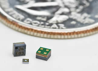 Akustica, developer of silicon MEMS (micro electro-mechanical systems) microphones for the consumer electronics market has been bought by Robert Bosch North America. Terms of the agreement will not be disclosed.
Akustica, which was founded in 2001, is based in Pittsburgh, Pennsylvania and develops and sells digital and analogue micro electromechanical microphones using standard CMOS silicon technology. This approach allows the integration of transducer elements and associated integrated circuits on a single Silicon chip. Bosch is the world leader in MEMS sensors and, with this acquisition, further strengthens its position in this market.
“The strategic acquisition of Akustica with their outstanding application of sophisticated MEMS technology complements our growing semiconductor business and ideally complements our ongoing MEMS activities” said Dr. Stefan Kampmann, executive vice president, Bosch Automotive Electronics. “We look forward to working together with the Akustica team to continue to develop this important business area.”
To date Akustica, which developed and sold the world’s first digital MEMS microphone, has sold over 5 million microphones in the global market. All of the company’s 36 associates will be employed by Bosch.
According to Joseph A. Jacobson, president and chief executive officer, Akustica, Inc., “We are excited to join the market leader in MEMS sensors and be a part of Bosch's expansion in commercialization of consumer MEMS products. The strength of our combined technology, manufacturing capability, and talent will allow us to continue delivering innovative and differentiating sensor product solutions.”
Comment: However, this looks more like the inability of Akustica to raise more money in the current financial climate and not enough income to go it alone despite big early plans.

Customer continuity is key says GE Fanuc
GE Fanuc has strongly objected to the idea that the joint venture has collapsed (see blog below), saying this is a strategic move based on changes in the market over the last twenty years. But it does not release turnover details for the joint venture, and with its focus on industrial and process control the joint venture is likely to be suffering as much as any other large equipment supplier.
The company does point to an amicable separation and the two parts will continue to work together to provide continuity for customers.
The two will continue to work together in motion control applications.
Comments?

The company does point to an amicable separation and the two parts will continue to work together to provide continuity for customers.
"The market place has changed, everything has changed since the joint venture was formed twenty three years ago," said a senior spokesperson at GE Fanuc. "One good example is the embedded business that is now a large part of GE. That's what is behind the dissolving, not the collapse, of the joint venture. This is a strategic decision so that both companies can refocus their interests for growth."
GE Fanuc acquired SBS Technologies, which had itself grown fast, and Radstone Technologies, in 2006, the latter for £130m, paying peak prices that I would expect not to be reflecting the same forward earnings in the current climate.
"This is not related to the downturn in the economy, but the downturn has made everyone focus on their business to see what they should focus on as the recovery occurs," said the spokesperson.
The two will continue to work together in motion control applications.
Comments?
Wireless power standard emerges with logo

A standard for wireless charging of portable equipment is emerging through the Wireless Power Consortium. It has released the 0.95 technical specification for a global wireless power charging standard for low power devices that are 5 watts and below, such as mobile phones and personal music players. It is out for review by its members and announced the launch of prototype testing at a members' interoperability test to be held on 15-17 September, 2009.
The Consortium, established at the end of last year, has also chosen the logo “Qi” (pronounced “chee”, meaning “energy flow”) to represent the first international wireless power standard which brings new levels of convenience to power charging in consumer electronic devices.
“In just seven months the Wireless Power Consortium has advanced the standard to 0.95 for interoperability testing and moved to trademark “Qi” as the first universal wireless power standard. These significant milestones have been achieved through strong collaboration among the Consortium members and pave the way for an accelerated 1.0 release schedule of the standard,” said Camille Tang, Co-Chair of the Promotion Work Group at the consortium.
The interoperability test will be hosted in Eindhoven, The Netherlands, during the next Consortium meeting and is open to existing and new members joining prior to 15 September 2009.
In a recent survey by the consortium 90% of respondents said they would like to see a uniform symbol placed on electronic devices to indicate that the devices are equipped with wireless power charging. Under the consortium’s plans, all electronic devices bearing the “Qi” symbol can be charged on any charging pad or surface marked with the same “Qi” logo.
Full members:
ConvenientPower
Fulton Innovation
Logitech
National Semiconductor
Olympus
Philips
Sang Fei
Sanyo
Texas Instruments
ASSOCIATE MEMBERS
Duracell
Hosiden
Leggett & Platt
Samsung Electronics
ST-Ericsson

Tuesday, August 18, 2009
Downturn hits as GE Fanuc splits
GE Fanuc Automation, the twenty year old joint venture between GE and FANUC, is to be dismantled by the end of the year. GE and FANUC expect the transaction to be completed by the end of this year, subject to satisfactory customary closing conditions. It denies the split is due to market conditions, see comments above.
Set up in 1986, GE Fanuc Automation serves a vast array of industries around the world including the energy, water, consumer packaged goods, government & defence, and telecommunications industries with hardware and software solutions, services, automation and embedded computing systems.
Under the terms of the agreement GE retains the software, services, embedded systems and control systems businesses globally. The company will be known as GE Intelligent Platforms, and will be led by GE Fanuc Intelligent Platforms CEO Maryrose Sylvester. FANUC retains the global CNC business.

Set up in 1986, GE Fanuc Automation serves a vast array of industries around the world including the energy, water, consumer packaged goods, government & defence, and telecommunications industries with hardware and software solutions, services, automation and embedded computing systems.
Under the terms of the agreement GE retains the software, services, embedded systems and control systems businesses globally. The company will be known as GE Intelligent Platforms, and will be led by GE Fanuc Intelligent Platforms CEO Maryrose Sylvester. FANUC retains the global CNC business.
FANUC Honorary Chairman Dr. Seiuemon Inaba said, “Our joint venture has achieved great success toward its original mission, which was to cooperate on the global growth and technical development of the PLC and CNC business. Over this time period, markets and opportunities also have changed dramatically, and both companies further expanded into adjacent segments. Today’s market conditions are such that it’s imperative we pursue these expanded opportunities, and while we have achieved great things together, it’s in both our best interests that we focus our efforts on industry opportunities unique to our respective companies and that will deliver greater benefits to both our companies.”
GE Fanuc Intelligent Platforms CEO Maryrose Sylvester said, "GE could not have asked for better partners than Dr. Inaba and FANUC. GE is proud of what our companies have achieved together - both the industry expertise and success across our product portfolios. For GE, this change will mean a continued, intense focus on serving our customers around the world while continuing to invest in significant growth platforms like process control systems, enterprise and automation software and embedded computing as we continue to build further expertise around the GE vertical infrastructure segments."
“Our top priority is a smooth completion of transition and continuity for all customers, business partners and employees. We are committed to delivering our customer commitments in every segment of our business."
Friday, August 07, 2009
First European 1Gb/s Internet
Zon Multimedia in Portugal is planning to launch a 1Gbit/s Internet service in September, reports Julian Clover at Cable TV Europe and other sources.
This is a phenomenal rise in speeds, and will put pressure on other providers across Europe who have been talking about 100Mbit/s, which Zon launched in January.
The system, which runs over cable, has already been field tested.
These speeds will drive a whole new class of Internet connected services and devices over the next two to three years.

This is a phenomenal rise in speeds, and will put pressure on other providers across Europe who have been talking about 100Mbit/s, which Zon launched in January.
The system, which runs over cable, has already been field tested.
These speeds will drive a whole new class of Internet connected services and devices over the next two to three years.
Wednesday, August 05, 2009
Linux and Nucleus for Marvell Sheeva chip
Mentor Graphics has developed a combined open-source Linux and Nucleus operating system (OS) solution for the Marvell Sheeva MV78200 Dual-core Embedded Processor.
This dual operating system support was co-developed by Mentor and Marvell for low power devices such as network controllers, switches and routers, high-performance storage, enterprise printers, DVRs, NVRs and video surveillance, and high-volume SMB gateways.
The MV78200 is a dual-core, high-performance, low-power, highly-integrated processor with the Marvell Sheeva CPU cores. Built on Marvell’s innovative Discovery system controller platform, the MV78200 is a complete System-on-Chip (SoC) solution, optimized for low power operation and ideally suited to a wide range of applications ranging from sophisticated routers, switches and wireless base stations to high-volume laser printer applications. Developers can use the dual OSs to manage separate functional requirements, yet allow them to easily and reliably communicate with each other. Mentor’s Nucleus OS is a fast, scalable and deterministic OS that can be used for operational tasks such as those required in printing drums and ink coverage for enterprise printers, whereas the Linux OS would be used for user interaction and communication.

This dual operating system support was co-developed by Mentor and Marvell for low power devices such as network controllers, switches and routers, high-performance storage, enterprise printers, DVRs, NVRs and video surveillance, and high-volume SMB gateways.
“Our collaboration with Mentor Graphics’ embedded systems team has allowed Marvell to address the multi-OS needs of our customers using dual-core processors,” said Dr Simon Milner, vice president and general manager of the Enterprise Business Unit, Consumer and Communications Business Group at Marvell Semiconductor. “The performance and real time qualities of Mentor’s Nucleus OS complement the power and flexibility of Linux, while their tools and services give our mutual customers a boost in product development.”
The MV78200 is a dual-core, high-performance, low-power, highly-integrated processor with the Marvell Sheeva CPU cores. Built on Marvell’s innovative Discovery system controller platform, the MV78200 is a complete System-on-Chip (SoC) solution, optimized for low power operation and ideally suited to a wide range of applications ranging from sophisticated routers, switches and wireless base stations to high-volume laser printer applications. Developers can use the dual OSs to manage separate functional requirements, yet allow them to easily and reliably communicate with each other. Mentor’s Nucleus OS is a fast, scalable and deterministic OS that can be used for operational tasks such as those required in printing drums and ink coverage for enterprise printers, whereas the Linux OS would be used for user interaction and communication.
China chip market booms

China's IC market is expected to reach $100.1 billion in 2013 and represent over one-third (35%) of the worldwide IC market, up from only 14 in 2003 (Figure 1) according to IC Insights Mid-Year Update to The McClean Report.
In 2001, the Asia-Pacific IC market (which includes China, Taiwan, Singapore, Korea, etc.) first surpassed the Americas segment (the U.S., Canada, Mexico, Central America, and South America) and became the leading IC-consuming market.
In 2008, the Asia-Pacific IC market was $111.2 billion, and, for the first time ever, was larger than the Americas, European, and Japanese IC markets combined!
The tremendous growth of the Asia-Pacific IC market over the past few years mirrors the trend toward increasing electronic system production in the Asia-Pacific region, especially in China. In general, regional IC market growth is typically closely matched to the growth of regional electronic system production.
With more of the world's electronic systems forecast to be produced in Asia-Pacific (non-Japan), and China in particular, IC Insights believes that Asia-Pacific IC market growth will continue to significantly outpace total IC market growth for at least the next five years.
In 2009, China and Taiwan together are expected to represent about 75% of the IC market in the Asia-Pacific region. In 2013, IC Insights forecasts that the China and Taiwan IC market together will reach about $139 billion and represent almost 80% of the total Asia-Pacific IC market and almost half (48%) of the worldwide IC market!
In 2008, China's IC market increased 5% to $56.2 billion as compared to a 6% decline for the total worldwide IC market. Although China's IC market is forecast to decline by 8% in 2009, this performance would still be much better than the 17% drop expected for the total IC market. Moreover, the Chinese IC market is forecast to have a 2008-2013 CAGR of 12%, double the 6% forecast for the worldwide IC market during this same time.
Tuesday, August 04, 2009
High speed 64Gbyte memory cards emerge
Looking back even a couple of years, the prospect of using a 64Gbyte memory card for storage would seem fantastic, but Toshiba is planning to ship such cards, using the latest SDXC standard, to OEMs in November.
The new SDXC and 32Gbyte and 16Gbyte SDHC Memory Cards are the world’s first memory cards compliant with the SD Memory Card Standard Ver. 3.00, UHS104, which brings a new level of high speed read and write speeds to NAND flash based memory cards: a maximum write speed of 35MByte per second, and a read speed of 60MByte per second. For example, it would be possible to download 2.4GB video data in only 70 seconds.
SDXC Memory Card is the next-generation SD Memory Card standard defined by the SD Association in April 2009, in order to meet the ever-growing demand for high-capacity memory media, offering higher transfer rates for content rich storage applications. The new SDXC Memory Card Standard applies to cards with capacities over 32GB and up to 2Terabytes compared to the SDHC standard, which applies to cards with capacities from 4GB to 32GB. Like the move from SD to SDHC, the new cards are only compatible with SDXC readers, not existing SDHC systems.
UHS 104 is the new ultra high speed interface that delivers data at a rate of 104MB/ sec. It is the highest standard in the new SD Memory Card Standard Ver. 3.00.


The new SDXC and 32Gbyte and 16Gbyte SDHC Memory Cards are the world’s first memory cards compliant with the SD Memory Card Standard Ver. 3.00, UHS104, which brings a new level of high speed read and write speeds to NAND flash based memory cards: a maximum write speed of 35MByte per second, and a read speed of 60MByte per second. For example, it would be possible to download 2.4GB video data in only 70 seconds.
SDXC Memory Card is the next-generation SD Memory Card standard defined by the SD Association in April 2009, in order to meet the ever-growing demand for high-capacity memory media, offering higher transfer rates for content rich storage applications. The new SDXC Memory Card Standard applies to cards with capacities over 32GB and up to 2Terabytes compared to the SDHC standard, which applies to cards with capacities from 4GB to 32GB. Like the move from SD to SDHC, the new cards are only compatible with SDXC readers, not existing SDHC systems.
UHS 104 is the new ultra high speed interface that delivers data at a rate of 104MB/ sec. It is the highest standard in the new SD Memory Card Standard Ver. 3.00.

Wireless test and virtualisation for LabView 2009

National Instruments has launched its the latest version of the LabView graphical system design software platform for test, control and embedded system development. LabVIEW 2009 simplifies the development challenges of complex test systems with new tools that streamline the software engineering process for the development, deployment and maintenance of critical test software. It uses parallel programming features such as virtualisation technology that increase the performance for multicore-enabled test applications and offers LabVIEW FPGA compiler improvements to simplify field-programmable gate array (FPGA) reconfigurable I/O (RIO) development. In addition, LabVIEW provides new solutions for testing systems based on wireless standards such as WLAN, WiMAX, GPS and MIMO using a common hardware platform.
“In today’s challenging economic climate, engineers and scientists are being asked to complete their projects with fewer resources and in less time,” said Dr. James Truchard, President, CEO and Cofounder of National Instruments. “With LabVIEW 2009, test engineers can develop complex and mission-critical applications faster while improving their overall test system performance.”
Streamline Test Software Validation
LabVIEW 2009 features new tools for software engineering and code validation that make it possible for engineers and scientists to easily meet the regulatory and software engineering requirements of complex test systems. With the new version of LabVIEW, engineers and scientists can trace the implementation of test system requirements to virtual instrument (VI) programs and easily monitor low-level details about the execution of critical VIs for quick application monitoring and debugging. In addition, LabVIEW 2009 can automate the functional testing of each VI to guarantee that the VIs meet all necessary specifications. These new software engineering tools complement existing LabVIEW features for large application development and help engineers and scientists create high-quality test systems.
Improve Parallel System Development
With LabVIEW 2009, engineers and scientists can easily develop applications that take advantage of inherently parallel technologies such as FPGAs and multicore processors. Virtualisation technology makes it possible to run multiple OSs side by side on the same multicore processing hardware to build more efficient systems. Using new NI Real-Time Hypervisor software, engineers and scientists can run Windows XP and LabVIEW Real-Time OSs side by side on the same PXI embedded controller and partition the processor cores among the two OSs for more efficient use of system resources.
The LabVIEW 2009 FPGA Module also further reduces the time required to program FPGA RIO devices by providing early compile feedback and critical path highlighting during compilation and simulation on a development computer. This helps engineers and scientists make early FPGA resource usage estimates and better debug timing violations. They also can further reduce development time by simulating the behavior of an FPGA on a development computer instead of compiling to the FPGA.
Test More Wireless Devices and Standards
LabVIEW 2009 improves the performance of radio frequency (RF) and wireless test by taking advantage of multicore processors. For example, engineers and scientists can use LabVIEW and off-the-shelf multicore processors to increase the speed of wireless measurements such as spectral masks and error vector magnitude used in WLAN test. The recently released NI WLAN Measurement Suite for LabVIEW guarantees compliance with IEEE 802.11 a/b/g standards and performs measurements more than five times faster than traditional box instruments. With software-defined instrumentation using LabVIEW, engineers and scientists can implement the same measurement platform to generate, analyse and simulate nearly any wireless standard or custom protocol. In addition to the WLAN Measurement Suite, the recently released WiMAX, GPS and MIMO tools for LabVIEW help engineers and scientists increase their performance when testing multiple standards using a common PXI hardware platform.

Sunday, August 02, 2009
Google data on spring cleaning solar panels
Google has been looking at whether it should clean its solar panels, and d'uh, finds that the efficiency rises dramatically when it does! However, there are also some interesting slides on the data they collected.

Ever since we assembled a 1.6 MW solar panel installation at our headquarters in Mountain View in 2007, we've been wondering, "Does cleaning the solar panels make them more effective?" We thought it might, but we needed to be sure. So we analyzed the mountains of data that we collect about the energy that these panels produce — after rain, after cleaning and at different times of the year.
We have two different sets of solar panels on our campus — completely flat ones installed on carports, and rooftop ones that are tilted.
Since the carport solar panels have no tilt, rain doesn't do a good job of rinsing off the dirt they collect. (Also, our carports are situated across from a sand field, which doesn't help the situation.) We cleaned these panels for the first time after they had been in operation for 15 months, and their energy output doubled overnight. When we cleaned them again eight months later, their output instantly increased by 36 percent. In fact, we found that cleaning these panels is the #1 way to maximize the energy they produce. As a result, we've added the carport solar panels to our spring cleaning checklist.
The rooftop solar panels are a different story. Our data indicates that rain does a sufficient job of cleaning the tilted solar panels. Some dirt does accumulate in the corners, but the resulting reduction in energy output is fairly small — and cleaning tilted panels does not significantly increase their energy production. So for now, we'll let Mother Nature take care of cleaning our rooftop panels.
Accumulated dirt in the corners of a rooftop solar panel
We've also been crunching numbers on dollars-and-cents; the more energy our panels produce, the sooner we'll be paid back by our solar investment. Our analysis now predicts that Google's system will pay for itself in about six and a half years, which is even better than we initially expected.
If you want to learn more about our solar study, check out these slides showing the effects that seasonality, tilt, dirt, particulate matter, rain and cleaning have on Google's solar energy output. We hope you solar panel owners out there can tailor our analysis to the specifics of your own installation to produce some extra energy of your own!
Thursday, July 30, 2009
Printable electronics centre sees £20m boost
The Printable Electronics Technology Centre (Petec) near Durham, UK, is to get £20 million to expand its facility and services. The centre, at NETPark in Sedgfield, will receive £12 million from the UK Government’s Advanced Manufacturing strategy, and £8 million from the Regional Development Agency – One North East.
The funding will add new equipment for prototyping applications in:
* printable photovoltaics
* ultra-efficient lighting
* printable flexible displays
* new intelligent packaging
The new investment will also result in:
* 500m2 of new hi-tech equipment space for large-area application and production of pilot product manufacturing
* The development of new applications and knowledge which will attract new companies to the UK
* New private sector investment into novel lighting and solar energy harvesting applications
* Key technology applications in wide-area displays, photovoltaic generation, novel lighting and smart packaging by stimulating collaborations with new companies and linking with academia
* The development of a regional and UK-wide display, lighting and photovoltaic supply chain
* The work on Photovoltaic Cells and energy-efficient Organic Solid State lighting is also further investment in the North East’s new low-carbon industries, following announcements this month in projects covering wave power, biofuels, electric vehicles and industrial biotechnology
In the next four years it is estimated that this investment will stimulate the creation of up to 250 jobs in the North East and up to 1,500 jobs nationally.

The funding will add new equipment for prototyping applications in:
* printable photovoltaics
* ultra-efficient lighting
* printable flexible displays
* new intelligent packaging
The new investment will also result in:
* 500m2 of new hi-tech equipment space for large-area application and production of pilot product manufacturing
* The development of new applications and knowledge which will attract new companies to the UK
* New private sector investment into novel lighting and solar energy harvesting applications
* Key technology applications in wide-area displays, photovoltaic generation, novel lighting and smart packaging by stimulating collaborations with new companies and linking with academia
* The development of a regional and UK-wide display, lighting and photovoltaic supply chain
* The work on Photovoltaic Cells and energy-efficient Organic Solid State lighting is also further investment in the North East’s new low-carbon industries, following announcements this month in projects covering wave power, biofuels, electric vehicles and industrial biotechnology
In the next four years it is estimated that this investment will stimulate the creation of up to 250 jobs in the North East and up to 1,500 jobs nationally.
"One North East has been investing in PETEC for some time now, having identified printable electronics as one of the emerging industries that can drive the region’s economy forward," said Alan Welby, Director of Strategy at One North East. "The groundbreaking research and development work that has been taking place in Sedgefield is fast approaching a stage where it can become an area of major industrial growth and job creation for North East England."
Wednesday, July 29, 2009
Reconfigurable computing sees giant launch
With 96 high end FPGAs and 26 quad-core Nehalem Xeon processors, the world's largest and most powerful reconfigurable computer has been launched at the University of Florida.
Novo-G uses 96 Altera Stratix-III E260 devices, each with 768 18x18 multipliers, 254K logic elements and 204K registers, with 4.25GB of memory attached. These are housed in 24 GiDEL ProcStar-III quad-FPGA boards and supported by the 26 quad-core processors, 20Gb/s non-blocking DDR InfiniBand, GigE, and 576GB total RAM.
Novo-G will support a variety of tools, including vendor tools as well as various CHREC tools for formulation, design, translation, and execution. At the device level, Novo-G of course supports applications design with VHDL and Verilog, but also several high level ESL programming languages.
CHREC research equipment features a broad assortment of high-end FPGAs, accelerator boards, servers, clusters, and scalable systems. RC resources include those from AlphaData (boards), Altera (devices, boards, tools), Celoxica (boards), Cray (machines), DRC (machine, module), GiDEL (boards, tools), Nallatech (boards, cluster, tools), Pico Computing (boards), SGI (machines), SRC (machines), Tilera (GFE board), Xilinx (devices, boards, tools), and XtremeData (machines, modules).

Novo-G uses 96 Altera Stratix-III E260 devices, each with 768 18x18 multipliers, 254K logic elements and 204K registers, with 4.25GB of memory attached. These are housed in 24 GiDEL ProcStar-III quad-FPGA boards and supported by the 26 quad-core processors, 20Gb/s non-blocking DDR InfiniBand, GigE, and 576GB total RAM.
“Construction has been completed on the new Novo-G machine and it is now ready to support a variety of research experiments in CHREC for various projects and participants,” said Dr. Alan D. George, Professor of ECE and Director of the NSF Centre for High-performance Reconfigurable Computing (CHREC) at the University of Florida. “Novo-G is believed to be the most powerful reconfigurable computer in the known world, certainly at least the academic/research community and the FPGAs featured in Novo-G are among the most powerful available today.”
“Although Novo-G may at first sound like it only serves as a research machine in the HPC realm of reconfigurable computing (RC), in reality it supports equally well the HPEC (embedded) realm of RC,” he said. “The boards featured in Novo-G (GiDEL ProcStar-III) are themselves originally marketed and intended as embedded processing boards, each with four big FPGAs with many attached memory banks plus various other supporting devices. We happen to be putting and using more of them in a single machine than anyone has attempted before and researchers can focus on issues with a single FPGA, a set of two, three, or four FPGAs on a single board with fast streaming pipes between, or many FPGAs (up to 96) spanning multiple boards, as their needs require. Thus, Novo-G will be supporting RC research projects that span the HPC and HPEC sides.
Novo-G will support a variety of tools, including vendor tools as well as various CHREC tools for formulation, design, translation, and execution. At the device level, Novo-G of course supports applications design with VHDL and Verilog, but also several high level ESL programming languages.
“We have successfully ported the Impulse-C tool to this platform, the Altera FP Compiler is already in use in our work, and efforts are in progress to do the same for Mitrion-C, all with help from the board and associated tool vendors,” said Dr George “Efforts are in the works to port our CHREC performance tool (ReCAP) and its debug/verification sidekick to Novo-G, and our folks on RCML, Intermediate Fabrics, etc. also have plans for Novo-G.”
CHREC research equipment features a broad assortment of high-end FPGAs, accelerator boards, servers, clusters, and scalable systems. RC resources include those from AlphaData (boards), Altera (devices, boards, tools), Celoxica (boards), Cray (machines), DRC (machine, module), GiDEL (boards, tools), Nallatech (boards, cluster, tools), Pico Computing (boards), SGI (machines), SRC (machines), Tilera (GFE board), Xilinx (devices, boards, tools), and XtremeData (machines, modules).
Subscribe to:
Posts (Atom)